
Datasheet

LT1117/LT1117-2.85
LT1117-3.3/LT1117-5
8
1117fd
APPLICATIONS INFORMATION
Output Voltage
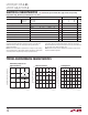
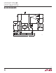
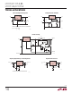
The LT1117 develops a 1.25V reference voltage between the
output and the adjust terminal (see Figure 2). By placing a
resistor between these two terminals, a constant current
is caused to flow through R1 and down through R2 to
set the overall output voltage. Normally this current is
chosen to be the specified minimum load current of 10mA.
Because I
ADJ
is very small and constant when compared
to the current through R1, it represents a small error and
can usually be ignored. For fixed voltage devices R1 and
R2 are included in the device.
1117 F02
R2
R1
V
OUT
V
IN
V
REF
I
ADJ
50µA
LT1117
IN
ADJ
OUT
V
OUT
= V
REF
1 + + I
ADJ
R2
R2
—
R1
+
Figure 2. Basic Adjustable Regulator
Load Regulation
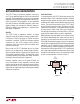
Because the LT1117 is a 3-terminal device, it is not possible
to provide true remote load sensing. Load regulation will be
limited by the resistance of the wire connecting the regulator
to the load. The data sheet specification for load regulation
is measured at the output pin of the device. Negative side
sensing is a true Kelvin connection, with the bottom of the
output divider returned to the negative side of the load.
Although it may not be immediately obvious, best load
regulation is obtained when the top of the resistor divider
(R1) is returned directly to the output pin of the device,
not to the load. This is illustrated in Figure 3. Connected
as shown, R
P
is not multiplied by the divider ratio. If R1
were connected to the load, the effective resistance between
the regulator and the load would be:
R
RR
R
R
PP
×
+
=
21
1
, Parasitic Line Resistance
1117 F03
R2
R1
V
IN
R
P
PARASITIC
LINE RESISTANCE
R
L
CONNECT
R1 TO CASE
CONNECT
R2 TO LOAD
LT1117
IN
ADJ
OUT
Figure 3. Connections for Best Load Regulation
For fixed voltage devices the top of R1 is internally Kelvin
connected, and the ground pin can be used for negative
side sensing.
Thermal Considerations
LT1117 series regulators have internal thermal limiting
circuitry designed to protect the device during overload
conditions. For continuous normal load conditions however,
the maximum junction temperature rating of 125°C must
not be exceeded.
It is important to give careful consideration to all sources
of thermal resistance from junction to ambient. For
the SOT-223 package, which is designed to be surface
mounted, additional heat sources mounted near the device
must also be considered. Heat sinking is accomplished
using the heat spreading capability of the PC board and
its copper traces. The thermal resistance of the LT1117 is
15°C/W from the junction to the tab. Thermal resistances
from tab to ambient can be as low as 30°C/W. The total
thermal resistance from junction to ambient can be as low
as 45°C/W. This requires a reasonable sized PC board with
at least one layer of copper to spread the heat across the
board and couple it into the surrounding air.