
Datasheet
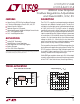

LT1117/LT1117-2.85
LT1117-3.3/LT1117-5
9
1117fd
APPLICATIONS INFORMATION
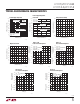
Experiments have shown that the heat spreading copper
layer does not need to be electrically connected to the
tab of the device. The PC material can be very effective at
transmitting heat between the pad area, attached to the
tab of the device, and a ground plane layer either inside
or on the opposite side of the board. Although the actual
thermal resistance of the PC material is high, the Length/
Area ratio of the thermal resistor between layers is small.
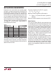
The data in Table 1 was taken using 1/16" FR-4 board with
1oz. copper foil. It can be used as a rough guideline in
estimating thermal resistance.
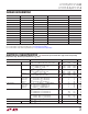
Table 1.
COPPER AREA
BOARD AREA
THERMAL RESISTANCE
(JUNCTION-TO-AMBIENT)TOPSIDE* BACKSIDE
2500 Sq. mm 2500 Sq. mm 2500 Sq. mm 45°C/W
1000 Sq. mm 2500 Sq. mm 2500 Sq. mm 45°C/W
225 Sq. mm 2500 Sq. mm 2500 Sq. mm 53°C/W
100 Sq. mm 2500 Sq. mm 2500 Sq. mm 59°C/W
1000 Sq. mm 1000 Sq. mm 1000 Sq. mm 52°C/W
1000 Sq. mm 0 1000 Sq. mm 55°C/W
* Tab of device attached to topside copper
The thermal resistance for each application will be
affected by thermal interactions with other components
on the board. Some experimentation will be necessary to
determine the actual value.
The power dissipation of the LT1117 is equal to:
P
D
= ( V
IN
– V
OUT
)( I
OUT
)
Maximum junction temperature will be equal to:
T
J
= T
A(MAX)
+ P
D
(Thermal Resistance (junction-to-
ambient))
Maximum junction temperature must not exceed 125°C.
Ripple Rejection
The curves for Ripple Rejection were generated using
an adjustable device with the adjust pin bypassed. These
curves will hold true for all values of output voltage. For
proper bypassing, and ripple rejection approaching the
values shown, the impedance of the adjust pin capacitor,
at the ripple frequency, should be < R1. R1 is normally in
the range of 100Ω to 200Ω. The size of the required adjust
pin capacitor is a function of the input ripple frequency. At
120Hz, with R1 = 100Ω, the adjust pin capacitor should
be >13µF. At 10kHz only 0.16µF is needed.
For fixed voltage devices, and adjustable devices without
an adjust pin capacitor, the output ripple will increase as
the ratio of the output voltage to the reference voltage
(V
OUT
/V
REF
). For example, with the output voltage equal
to 5V, the output ripple will be increased by the ratio of
5V/1.25V. It will increase by a factor of four. Ripple
rejection will be degraded by 12dB from the value shown
on the curve.