
Datasheet


3
LT1118/LT1118-2.5
LT1118-2.85/LT1118-5
1118fc
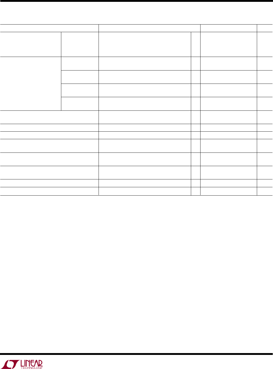
PARAMETER CONDITIONS MIN TYP MAX UNITS
Line Regulation (Note 4) LT1118 I
L
= 0mA, 4.2V ≤ V
IN
≤ 15V ● 6mV
LT1118-2.5 I
L
= 0mA, 4.2V ≤ V
IN
≤ 15V ● 6mV
LT1118-2.85 I
L
= 0mA, 4.75V ≤ V
IN
≤ 15V ● 6mV
LT1118-5 I
L
= 0mA, 6.5V ≤ V
IN
≤ 15V ● 10 mV
Load Regulation (Note 4) LT1118 0mA ≤ I
L
≤ 800mA ● 6mV
–400mA ≤ I
L
≤ 0mA ● 6mV
LT1118-2.5 0mA ≤ I
L
≤ 800mA ● 12 mV
–400mA ≤ I
L
≤ 0mA ● 12 mV
LT1118-2.85 0mA ≤ I
L
≤ 800mA ● 12 mV
–400mA ≤ I
L
≤ 0mA ● 12 mV
LT1118-5 0mA ≤ I
L
≤ 800mA ● 25 mV
–400mA ≤ I
L
≤ 0mA ● 25 mV
Dropout Voltage (Note 5) I
L
= 100mA 0.85 1.1 V
I
L
= 800mA 1 1.3 V
FB Pin Bias Current LT1118 0.35 1 µA
Minimum Output Voltage LT1118 ● 2.1 V
Ripple Rejection f
RIPPLE
= 120Hz, V
IN
– V
OUT
= 2V 60 80 dB
V
RIPPLE
= 0.5V
P-P
Load Transient Settling Time, 0mA ≤ I
L
≤ 800mA, C
LOAD
= 1µF5µs
∆V = 1% –400mA ≤ I
L
≤ 0mA, C
LOAD
= 1µF5µs
Output Short-Circuit Current I
SC
+
V
OUT
= 0V 800 1200 mA
I
SC
–
V
OUT
= V
IN
–700 –400 mA
Thermal Shutdown Junction Temperature No Load 170 °C
Enable Turn-On Delay No Load 50 µs
Note 1: Stresses beyond those listed under Absolute Maximum Ratings
may cause permanent damage to the device. Exposure to any Absolute
Maximum Rating condition for extended periods may affect device
reliability and lifetime.
Note 2: Unless otherwide specified, testing done at V
CC
= 5V
(LT1118-2.5, LT1118-2.85) or V
CC
= 7V (LT1118-5). V
EN
= V
CC
. Output
C
LOAD
= 1µF, I
LOAD
= 0.
Note 3: All operating conditions include the combined effects of load
current, input voltage and temperature over each parameter’s full range.
Note 4: Load and line regulation are tested at a constant junction
temperature by low duty cycle pulse testing.
Note 5: Dropout voltage is defined as the minimum input to output voltage
measured while sourcing the specified current.
ELECTRICAL CHARACTERISTICS
The ● denotes specifications which apply over the full operating temperature range, otherwise specifications are at T
A
= 25°C. (Note 2)