
Datasheet


LT1121/LT1121-3.3/LT1121-5
11
1121fg
APPLICATIONS INFORMATION
resistor is shown in Table 6. The LT1121 is a micropower
device and output transient response will be a function of
output capacitance. See the Transient Response curves
in the Typical Performance Characteristics. Larger values
of output capacitance will decrease the peak deviations
and provide improved output transient response. Bypass
capacitors, used to decouple individual components
powered by the LT1121, will increase the effective value
of
the output capacitor.
Protection Features
The LT1121 incorporates several protection features
which make it ideal for use in battery-powered circuits.
In addition to the normal protection features associated
with monolithic regulators, such as current limiting and
thermal limiting, the device is protected against reverse
input voltages, reverse output voltages, and reverse volt-
ages from output to input.
Current limit protection and thermal overload protection
are intended
to protect the device against current overload
conditions at the output of the device. For normal opera-
tion, the junction temperature should not exceed 125°C.
The input of the device will withstand reverse voltages of
30V. Current flow into the device will be limited to less
than 1mA (typically less than 100µA) and no negative
voltage will appear at the output. The device will protect
both
itself and the load. This provides protection against
batteries that can be plugged in backwards.
For fixed voltage versions of the device, the output can
be pulled below ground without damaging the device. If
the input is open circuit or grounded the output can be
pulled below ground by 20V. The output will act like an
open circuit, no current will flow out of the pin. If
the input
is powered by a voltage source, the output will source the
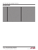
Table 6. Suggested Series Resistor Values
OUTPUT CAPACITANCE SUGGESTED SERIES RESISTOR
0.33µF
2Ω
0.47µF
1Ω
0.68µF
1Ω
>1µF None Needed
short-circuit current of the device and will protect itself by
thermal limiting. For the adjustable version of the device,
the output pin is internally clamped at one diode drop
below ground. Reverse current for the adjustable device
must be limited to 5mA.
In circuits where a backup battery is
required, several
different input/output conditions can occur. The output
voltage may be held up while the input is either pulled
to ground, pulled to some intermediate voltage, or is left
open circuit. Current flow back into the output will vary
depending on the conditions. Many battery-powered cir-
cuits incorporate some form of power management. The
following information will help optimize battery life. Table
7 summarizes the
following information.
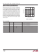
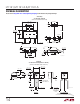
The reverse output current will follow the curve in Figure
2 when the input pin is pulled to ground. This current
flows through the output pin to ground. The state of the
shutdown pin will have no effect on output current when
the input pin is pulled to ground.
In some applications it may be necessary to leave the
input to the LT1121 unconnected when
the output is held
high. This can happen when the LT1121 is powered from
a rectified AC source. If the AC source is removed, then
the input of the LT1121 is effectively left floating. The
reverse output current also follows the curve in Figure 2
if the input pin is left open. The state of the shutdown pin
will have no effect on the reverse output current
when the
input pin is floating.
Figure 2. Reverse Output Current
OUTPUT VOLTAGE (V)
0
OUTPUT PIN CURRENT (μA)
100
90
80
70
60
50
40
30
20
10
0
8
1121• F02
2
4
6
10
1 3 5 7 9
T
J
= 25°C
V
IN
< V
OUT
CURRENT FLOWS
INTO OUTPUT PIN
TO GROUND
LT1121-3.3
LT1121
(V
OUT
= V
ADJ
)
LT1121-5