
Datasheet


LT1122
5
1122fb
For more information www.linear.com/LT1122
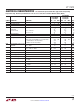
ELECTRICAL CHARACTERISTICS
Note 1: Stresses beyond those listed under Absolute Maximum Ratings
may cause permanent damage to the device. Exposure to any Absolute
Maximum Rating condition for extended periods may affect device
reliability and lifetime.
Note 2: The LT1122 is measured in an automated tester in less than one
second after application of power. Depending on the package used, power
dissipation, heat sinking, and air flow conditions, the fully warmed up chip
temperature can be 10°C to 50°C higher than the ambient temperature.
Note 3: Settling time is 100% tested for A- and C-grades using the settling
time test circuit shown. This test is not included in quality assurance
sample testing.
Note 4: Input voltage range functionality is assured by testing offset
voltage at the input voltage range limits to a maximum of 4mV
(A, B grades), to 5.7mV (C, D grades).
Note 5:
Minimum supply voltage is tested by measuring offset voltage to
7mV maximum at ±5V supplies.
Note 6: The LT1122 is not tested and not quality-assurance-sampled
at –40°C and at 85°C. These specifications are guaranteed by design,
correlation and/or inference from –55°C, 0°C, 25°C, 70°C and/or 125°C
tests.
16
15
14
13
12
11
10
9
8
7
6
5
4
3
2
1
15V
1µF TANT
0.1µF
1µF TANT
0.1µF
TYPICAL SUPPLY
BYPASSING FOR
EACH AMP/BUFFER
–10V
(REGULATED)
1
2
TTL
IN
4
5
74LS00
GROUND ALL
OTHER INPUTS
10V
(REGULATED)
6
3
SETTLING
TIME OUTPUT
(20 TIMES SUM
NODE OUTPUT)
1k
NO CONNECTION ON PINS
10, 11, 12, 14, AND 15
1N5712
15V
–15V
1.5k
LT1223
–
+
3
2
4
7
6
8
1
7
2
5
4
1N5712
SUMMING
NODE
OUTPUT
–15V
15V
*THIS RESISTOR CAN BE ADJUSTED TO
NULL OUT ALL OFFSETS AT THE SETTLING
TIME OUTPUT. THE AUTOMATED TESTER
USES A SEPARATE AUTOZERO CIRCUIT.
–15V
(MEASURE INPUT
PULSE HERE)
V
IN
5.1k
1%
4
–15V
3
2
7
6
LT1122
2k
1%
15V
2k
1%
DEVICE UNDER TEST
5pF
15V
7
1
5
2
8
51Ω
51Ω 51Ω
51Ω
+
–
HA5002
79Ω
5.1k*
1%
HA5002
4
LTC201A
LT1122•TA02
–15V
+
+
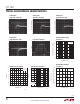
Settling Time Test Fixture