
Datasheet


LT1129/LT1129-3.3/LT1129-5
12
112935ff
APPLICATIONS INFORMATION
Current limit protection and thermal overload protection
are intended to protect the device against current overload
conditions at the output of the device. For normal operation,
the junction temperature should not exceed 125°C.
The input of the device will withstand reverse voltages
of 30V. Current fl ow into the device will be limited to less
than 1mA (typically less than 100μA) and no negative
voltage will appear at the output. The device will protect
both itself and the load. This provides protection against
batteries that can be plugged in backwards.
For fi xed voltage versions of the device, the sense pin
is internally clamped to one diode drop below ground.
For the adjustable version of the device, the output pin
is internally clamped at one diode drop below ground. If
the output pin of an adjustable device, or the sense pin
of a fi xed voltage device, is pulled below ground, with the
input open or grounded, current must be limited to less
than 5mA.
In circuits where a backup battery is required, several
different input/output conditions can occur. The output
voltage may be held up while the input is either pulled
to ground, pulled to some intermediate voltage, or is left
open circuit. Current fl ow back into the output will vary
depending on the conditions. Many battery-powered
circuits incorporate some form of power management.
The following information will help optimize battery life.
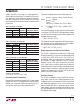
Table 4 summarizes the following information.
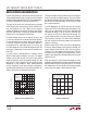
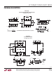
The reverse output current will follow the curve in Figure 3
when the input pin is pulled to ground. This current fl ows
through the output pin to ground. The state of the shutdown
pin will have no effect on output current when the input
pin is pulled to ground.
In some applications it may be necessary to leave the
input to the LT1129 unconnected when the output is held
high. This can happen when the LT1129 is powered from
a rectifi ed AC source. If the AC source is removed, then
the input of the LT1129 is effectively left fl oating. The
reverse output current also follows the curve in Figure 3
if the input pin is left open. The state of the shutdown pin
will have no effect on the reverse output current when the
input pin is fl oating.
When the input of the LT1129 is forced to a voltage below
its nominal output voltage and its output is held high, the
reverse output current will still follow the curve shown
in Figure 3. This can happen if the input of the LT1129 is
connected to a discharged (low voltage) battery and the
output is held up by either a backup battery or by a second
regulator circuit.
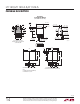
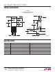
When the input pin is forced below the output pin or the
output pin is pulled above the input pin, the input current will
typically drop to less than 2μA (see Figure 4). The state of
the shutdown pin will have no effect on the reverse output
current when the output is pulled above the input.
OUTPUT VOLTAGE (V)
0
OUTPUT PIN CURRENT (μA)
100
90
80
70
60
50
40
30
20
10
0
8
112935 F03
2
4
6
10
13579
T
J
= 25°C
V
IN
= 0V
V
SENSE
= V
OUT
CURRENT FLOWS
INTO DEVICE
LT1129-3.3
LT1129
LT1129-5
Figure 3. Reverse Output Current
INPUT VOLTAGE (V)
0
INPUT CURRENT (μA)
5
4
3
2
1
0
4
112935 F04
1
2
3
5
V
OUT
= 3.3V (LT1129-3.3)
V
OUT
= 5V (LT1129-5)
Figure 4. Input Current