
Datasheet


LT1129/LT1129-3.3/LT1129-5
13
112935ff
Information furnished by Linear Technology Corporation is believed to be accurate and reliable.
However, no responsibility is assumed for its use. Linear Technology Corporation makes no representa-
tion that the interconnection of its circuits as described herein will not infringe on existing patent rights.
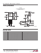
APPLICATIONS INFORMATION
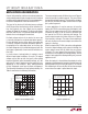
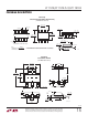
F Package
20-Lead Plastic TSSOP (4.4mm)
(LTC DWG # 05-08-1650)
OBSOLETE PACKAGE
F20 TSSOP 0204
0.09 – 0.20
(.0035 – .0079)
0° – 8°
0.25
REF
0.50 – 0.75
(.020 – .030)
4.30 – 4.50**
(.169 – .177)
134
5
6
7
8910
111214 13
6.40 – 6.60*
(.252 – .260)
20 19 18 17 16 15
1.10
(.0433)
MAX
0.05 – 0.15
(.002 – .006)
0.65
(.0256)
BSC
6.40
(.252)
BSC
0.19 – 0.30
(.0075 – .0118)
TYP
2
MILLIMETERS
(INCHES)
DIMENSIONS DO NOT INCLUDE MOLD FLASH. MOLD FLASH
SHALL NOT EXCEED .152mm (.006") PER SIDE
*
NOTE:
1. CONTROLLING DIMENSION: MILLIMETERS
2. DIMENSIONS ARE IN
3. DRAWING NOT TO SCALE
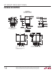
RECOMMENDED SOLDER PAD LAYOUT
0.45 ±0.05
0.65 BSC
4.50 ±0.10
6.60 ±0.10
1.05 ±0.10
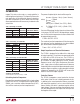
Table 4. Fault Conditions
INPUT PIN SHDN PIN OUTPUT PIN
< V
OUT
(Nominal) Open (Hi) Forced to V
OUT
(Nominal) Reverse Output Current ≈ 15μA (See Figure 3)
Input Current ≈ 1μA (See Figure 4)
< V
OUT
(Nominal) Grounded Forced to V
OUT
(Nominal) Reverse Output Current ≈ 15μA (See Figure 3)
Input Current ≈ 1μA (See Figure 4)
Open Open (Hi) Forced to V
OUT
(Nominal) Reverse Output Current ≈ 15μA (See Figure 3)
Open Grounded Forced to V
OUT
(Nominal) Reverse Output Current ≈ 15μA (See Figure 3)
PACKAGE DESCRIPTION