
Datasheet
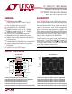


8
LT1130A/LT1140A Series
PI FU CTIO S
U
UU
V
–
: Negative Supply Output (RS232 Drivers). V
–
≈ –(2V
CC
– 2.5V). This pin requires an external charge storage
capacitor C ≥ 0.1µF. V
–
is short-circuit proof for
30 seconds.
C1
+
, C1
–
, C2
+
, C2
–
:
Commutating Capacitor Inputs.
These pins require two external capacitors C ≥ 0.2µF: one
from C1
+
to C1
–
, and another from C2
+
to C2
–
. To
maintain charge pump efficiency, the capacitor’s effective
series resistance should be less than 2Ω. For C ≥ 1µF, low
ESR tantalum capacitors work well in this application,
although small value ceramic capacitors may be used
with a minimal reduction in charge pump compliance. In
applications where larger positive voltages are available,
such as 12V, C1 may be omitted and the positive voltage
may be connected directly to the C1
+
pin. In this mode of
operation, the V
+
pin should be decoupled with a 0.1µF
ceramic capacitor.
DRIVER IN: RS232 Driver Input Pins. These inputs are
TTL/CMOS compatible. Inputs should not be allowed to
float. Tie unused inputs to V
CC
.
DRIVER OUT: Driver Outputs at RS232 Voltage Levels.
Driver output swing meets RS232 levels for loads up to 3k.
Slew rates are controlled for lightly loaded lines. Output
current capability is sufficient for load conditions up to
2500pF. Outputs are in a high impedance state when in
shutdown mode, V
CC
= 0V, or when the DRIVER DISABLE
pin is active. Outputs are fully short-circuit protected from
V
–
+ 30V to V
+
– 30V. Applying higher voltages will not
damage the device if the overdrive is moderately current
limited. Short circuits on one output can load the power
supply generator and may disrupt the signal levels of the
other outputs. The driver outputs are protected against
ESD to ±10kV for human body model discharges.
RX IN: Receiver Inputs. These pins accept RS232 level
signals (±30V) into a protected 5k terminating resistor.
The receiver inputs are protected against ESD to ±10kV for
human body model discharges. Each receiver provides
0.4V of hysteresis for noise immunity. Open receiver
inputs assume a logic low state.
RX OUT: Receiver Outputs with TTL/CMOS Voltage Lev-
els. Outputs are in a high impedance state when in shut-
down mode to allow data line sharing. Outputs are fully
short-circuit protected to ground or V
CC
with the power
on, off, or in shutdown mode.
ESD PROTECTIO
U
The RS232 line inputs of the LT1130A/LT1140A series of
RS232 Driver/Receivers have on-chip protection from
ESD transients up to ±10kV. The protection structures act
to divert the static discharge safely to system ground. In
order for the ESD protection to function effectively, the
power supply and ground pins of the LT1130A/LT1140A
must be connected to ground through low impedances.
The power supply decoupling capacitors and charge
pump storage capacitors provide this low impedance in
normal application of the circuit. The only constraint is
that low ESR capacitors must be used for bypassing and
charge storage. ESD testing must be done with pins V
CC
,
V
+
, V
–
and GND shorted to ground or connected with low
ESR capacitors.
The ESD protection on the LT1133A, LT1137A and
LT1141A meets ±15kV air gap discharge and ±8kV con-
tact methods per IEC-1000-4-2.
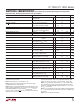
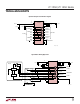
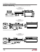
LT1130A • ESD TC
5V V
CC
0.1µF
0.2µF
0.1µF
RS232
LINE PINS
PROTECTED
TO ±15kV
LT1137A
1
2
3
4
5
6
7
8
9
10
11
12
13
14
DRIVER 1 OUT
RX1 IN
DRIVER 2 OUT
RX2 IN
RX3 IN
RX4 IN
DRIVER 3 OUT
RX5 IN
ON/OFF
28
27
26
25
24
23
22
21
20
19
18
17
16
15
0.2µF
DRIVER 1 IN
RX1 OUT
DRIVER 2 IN
RX2 OUT
RX3 OUT
RX4 OUT
DRIVER 3 IN
RX5 OUT
V
–
V
+
0.1µF
GND
DRIVER DISABLE
+
+
ESD Test Circuit