
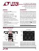
Datasheet

5
LT1130A/LT1140A Series
E
LECTR
IC
AL C CHARA TERIST
ICS
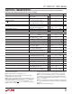
PARAMETER CONDITIONS MIN TYP MAX UNITS
Supply Current when OFF (V
CC
) Shutdown (Note 4) ● 110 µA
Driver Disable 4 mA
Supply Rise Time C1, C2, C
+
, C
–
= 1.0µF 2.0 ms
Shutdown to Turn-On C
+
, C
–
= 0.1µF, C1, C2 = 0.2µF 0.2 ms
ON/OFF Pin Thresholds Input Low Level (Device Shut Down) ● 1.4 0.8 V
Input High Level (Device Enabled)
● 2.4 1.4 V
ON/OFF Pin Current 0V ≤ V
ON/OFF
≤ 5V ● –15 80 µA
DRIVER DISABLE Pin Thresholds Input Low Level (Drivers Enabled) ● 1.4 0.8 V
Input High Level (Drivers Disabled)
● 2.4 1.4 V
DRIVER DISABLE Pin Current 0V ≤ V
DRIVER DISABLE
≤ 5V ● –10 500 µA
Oscillator Frequency 130 kHz
Any Driver
Output Voltage Swing Load = 3k to GND Positive ● 5 7.3 V
Negative
● –6.5 – 5 V
Logic Input Voltage Level Input Low Level (V
OUT
= High) ● 1.4 0.8 V
Input High Level (V
OUT
= Low) ● 2 1.4 V
Logic Input Current 0.8V ≤ V
IN
≤ 2V ● 520 µA
Output Short-Circuit Current V
OUT
= 0V ±9 ±17 mA
Output Leakage Current Shutdown V
OUT
= ±30V (Note 4) ● 10 100 µA
Data Rate R
L
= 3k, C
L
= 2500pF 120 kbaud
R
L
= 3k, C
L
= 1000pF 250 kbaud
Slew Rate R
L
= 3k, C
L
= 51pF 15 30 V/µs
R
L
= 3k, C
L
= 2500pF (Note 8) 6 V/µs
Propagation Delay Output Transition t
HL
High to Low (Note 5) 0.6 1.3 µs
Output Transition t
LH
Low to High 0.5 1.3 µs
Any Receiver
Input Voltage Thresholds Input Low Threshold (V
OUT
= High) ● 0.8 1.3 V
Input High Threshold (V
OUT
= Low) ● 1.7 2.4 V
Hysteresis ● 0.1 0.4 1 V
Input Resistance –10V < V
IN
< 10V 3 5 7 kΩ
Output Voltage Output Low, I
OUT
= –1.6mA ● 0.2 0.4 V
Output High, I
OUT
= 160µA (V
CC
= 5V) ● 3.5 4.2 V
Output Leakage Current Shutdown (Note 4) 0 ≤ V
OUT
≤ V
CC
● 110 µA
Output Short-Circuit Current Sinking Current, V
OUT
= V
CC
–20 –10 mA
Sourcing Current, V
OUT
= 0V 10 20 mA
Propagation Delay Output Transition t
HL
High to Low (Note 6) 250 600 ns
Output Transition t
LH
Low to High 350 600 ns
Note 1: Absolute Maximum Ratings are those values beyond which the life
of the device may be impaired.
Note 2: Testing done at V
CC
= 5V and V
ON/OFF
= 3V.
Note 3: Supply current is measured with driver and receiver outputs
unloaded and the driver inputs tied high.
Note 4: Supply current and driver leakage current measurements in shut-
down are performed with V
ON/OFF
= 0.1V. Supply current measurements
using DRIVER DISABLE are performed with V
DRIVER DISABLE
= 3V. For
LT1135, LT1139, LT1140 and LT1141 with 12V supplies, V
OUT
leakage is
200µA for V
OUT
forced to ±25V.
Note 5: For driver delay measurements, R
L
= 3k and C
L
= 51pF. Trigger
points are set between the driver’s input logic threshold and the output
transition to the zero crossing (t
HL
= 1.4V to 0V and t
LH
= 1.4V to 0V).
Note 6: F
or receiver delay measurements, C
L
= 51pF. Trigger points
are set between the receiver’s input logic threshold and the output
transition to standard TTL/CMOS logic threshold (t
HL
= 1.3V to 2.4V
and t
LH
= 1.7V to 0.8V).
Note 7: For LT1133A/LT1137A, absolute maximum externally applied
V
–
= –6.5V. Internal charge pump will drive this pin to a higher nega-
tive voltage.
Note 8: For LT1137A, 4V/µs minimum.
The ● denotes the specifications which apply over the full operating
temperature range, otherwise specifications are at T
A
= 25°C. (Note 2)