
Datasheet

7
LT1130A/LT1140A Series
CCHARA TERIST
ICS
UW
AT
Y
P
I
CA
LPER
F
O
R
C
E
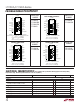
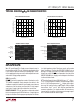
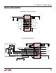
Shutdown to Driver Output
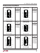
Receiver Short-Circuit Current
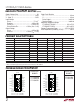
Driver Short-Circuit Current
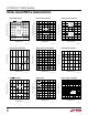
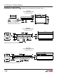
Driver Output Waveforms
LT1137A • TPC12
10
5
0
–10
–5
DRIVER OUTPUT
R
L
= 3k
C
L
= 2500pF
INPUT
DRIVER OUTPUT
R
L
= 3k
PI FU CTIO S
U
UU
V
CC
: 5V Input Supply Pin. Supply current drops to zero in
the shutdown mode. This pin should be decoupled with a
0.1µF ceramic capacitor close to the package pin. Insuffi-
cient supply bypassing can result in low output drive levels
and erratic charge pump operation.
GND: Ground Pin.
ON/OFF: Control the operation mode of the device and is
TTL/CMOS compatible. A logic low puts the device in the
shutdown mode which reduces input supply curent to zero
and places all of the drivers and receivers in high imped-
ance state. A logic high fully enables the transceiver.
DRIVER DISABLE: This pin provides an alternate control
for the charge pump and RS232 drivers. A logic high on
this pin shuts down the charge pump and places all drivers
in a high impedance state. Receivers remain active under
these conditions. Floating the DRIVER DISABLE pin or
driving it to a logic low level fully enables the transceiver.
A logic low on the ON/OFF pin supersedes the state of the
DRIVER DISABLE pin. Supply current drops to 4mA when
in driver disable mode.
V
+
: Positive Supply Output (RS232 Drivers). V
+
≈ 2V
CC
–
1.5V. This pin requires an external charge storage capaci-
tor C ≥ 1.0µF, tied to ground or V
CC
. Larger value capaci-
tors may be used to reduce supply ripple. With multiple
transceivers, the V
+
and V
–
pins may be paralleled into
common capacitors. For large numbers of transceivers,
increasing the size of the shared common storage capaci-
tors is recommended to reduce ripple.
TEMPERATURE (°C)
–55
SHORT-CIRCUIT CURRENT (mA)
20
25
30
25 75
LT1137A • TPC10
15
10
–25 0
50 100 125
5
0
ISC
+
ISC
–
TEMPERATURE (°C)
–55
0
SHORT-CIRCUIT CURRENT (mA)
20
50
0
50
75
LT1137A • TPC11
10
40
30
–25
25
100
125
ISC
+
ISC
–
LT1137A • TPC13
DRIVER
OUTPUT HIGH
R
L
= 3k
ON/OFF PIN
DRIVER
OUTPUT LOW
R
L
= 3k