
Datasheet


LT1175
8
1175ff
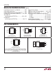
PIN FUNCTIONS
V
IN
(Pins 1, 8/Pin 3, Tab/Pin 2, Tab/Pins 1, 8/Pin 3, Tab):
Power is supplied to the device through this pin. A bypass
capacitor is required on this pin if the device is more than
six inches away from the main fi lter capacitor. In general,
the impedance of a battery rises with frequency, so it is
advisable to include a bypass capacitor in battery-powered
circuits. A 1μF or larger tantalum capacitor is suggested
for all applications, but if low ESR capacitors such as
ceramic or fi lm are used for the output and input capaci-
tors, the input capacitor should be three times the value
of the output capacitor.
I
LIM2
, I
LIM4
(Pins 2, 7/NA/NA/Pins 2, 7/NA): The two
current limit pins are emitter sections of the power transis-
tor. When left open, they fl oat several hundred millivolts
above the negative input voltage. When shorted to the
input voltage, they increase current limit by a minimum
of 200mA for I
LIM2
and 400mA for I
LIM4
. These pins must
be connected only to the input voltage, either directly or
through a resistor.
OUTPUT (Pin 3/Pin 1/Pin 1/Pin 3/Pin 1): The OUTPUT pin
is the collector of the NPN power transistor. It can be forced
to the input voltage, to ground or up to 2V positive with
respect to ground without damage or latchup (see Output
Voltage Reversal in Applications Information section). The
LT1175 has foldback current limit, so maximum current at
the OUTPUT pin is a function of input-to-output voltage.
See Typical Performance Characteristics.
SENSE (Pin 4/Pin 2/NA/Pin 4/Pin 2): The SENSE pin is
used in the adjustable version to allow custom selection
of output voltage, with an external divider set to generate
3.8V at the SENSE pin. Input bias current is typically 75nA
fl owing out of the pin. Maximum forced voltage on the
SENSE pin is 2V and –10V with respect to GND pin.
The fi xed 5V version utilizes the SENSE pin to give true
Kelvin connections to the load or to drive an external pass
transistor for higher output currents. Bias current out
of the 5V SENSE pin is approximately 12μA. Separating
the SENSE and OUTPUT pins also allows for a new loop
compensation technique described in the Applications
Information section.
GND (Pin 5/Pin 4/Pin 3/Pin 5/Pin 4): The GND pin has a
quiescent current of 45μA at zero load current, increas-
ing by approximately 10μA per mA of output current. At
500mA output current, GND pin current is about 5mA.
Current fl ows into the GND pin.
SHDN (Pin 6/Pin 5/NA/Pin 6/Pin 5): The SHDN pin is
specially confi gured to allow it to be driven from either
positive voltage logic or with negative only logic. Forc-
ing the SHDN pin 2V either above or below the GND
pin will turn the regulator on. This makes it simple to
connect directly to positive logic signals for active low
shutdown. If no positive voltages are available, the
SHDN pin can be driven below the GND pin to turn the
regulator on. When left open, the SHDN pin will default
low to a regulator “on” condition. For all voltages below
absolute maximum ratings, the SHDN pin draws only a
few microamperes of current (see Typical Performance
Characteristics). Maximum voltage on the SHDN pin is 15V,
–20V with respect to the GND pin and 35V, –5V with
respect to the negative input pin.
(N8/Q/ST/S8/T)