
Datasheet


5
LT1180A/LT1181A
11801afb
CCHARA TERIST
ICS
UW
AT
Y
P
I
CA
LPER
F
O
R
C
E
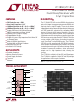
LOAD CAPACITANCE (nF)
0
SLEW RATE (V/µs)
12
16
4.0
LT1180A • TPC11
8
4
0
1.0
2.0
3.0
5.0
10
14
6
2
3.5
0.5
1.5
2.5
4.5
+SLEW
–SLEW
LT1180A • TPC13
LT1180A • TPC12
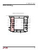
INPUT
DRIVER OUTPUT
R
L
= 3k
DRIVER OUTPUT
R
L
= 3k
C
L
= 2500pF
DRIVER 1
OUTPUT
ON/OFF PIN
Shutdown to Driver Outputs Driver Output Waveforms
10V
5V
GND
GND
–10V
–5V
DRIVER 2
OUTPUT
Slew Rate vs Load Capacitance
Receiver Short-Circuit Current
PI FU CTIO S
U
UU
V
+
: Positive Supply Output (RS232 Drivers). V
+
≈ 2V
CC
–
1.5V. This pin requires an external charge storage capaci-
tor C ≥ 0.1µF, tied to ground or V
CC
. Larger value capaci-
tors may be used to reduce supply ripple. With multiple
transceivers, the V
+
and V
–
pins may be paralleled into
common capacitors.
V
–
: Negative Supply Output (RS232 Drivers). V
–
≈ –(2V
CC
– 2.5V). This pin requires an external charge storage
capacitor C ≥ 0.1µF. Larger value capacitors may be used
to reduce supply ripple. With multiple transceivers, the V
+
and V
–
pins may be paralleled into common capacitors.
TEMPERATURE (°C)
–55
0
SHORT-CIRCUIT CURRENT (mA)
20
50
0
50
75
LT1180A • TPC10
10
40
30
–25
25
100
125
RX I
SC
–
RX I
SC
+
V
CC
: 5V Input Supply Pin. This pin should be decoupled
with a 0.1µF ceramic capacitor close to the package pin.
Insufficient supply bypassing can result in low output
drive levels and erratic charge pump operation.
GND: Ground Pin.
ON/OFF: A TTL/CMOS Compatible Operating Mode Con-
trol. A logic low puts the LT1180A in shutdown mode.
Supply current drops to zero and both driver and receiver
outputs assume a high impedance state. A logic high fully
enables the device.