
Datasheet


4
LT1203/LT1205
Note 2: The digital inputs (pins 5, 6 for the LT1203, pins 9, 10, 13, 14 for
the LT1205) are protected against ESD and overvoltage with internal
SCRs. For inputs ≤±6V the SCR will not fire. Voltages above 6V will fire
the SCR and the DC current should be limited to 50mA. To turn off the
SCR the pin voltage must be reduced to less than 2V or the current
reduced to less than 10mA.
Note 3: A heat sink may be required depending on the power supply
voltage.
Note 4: Commercial grade parts are designed to operate over the
temperature range of –40°C to 85°C but are neither tested nor guaranteed
beyond 0°C to 70°C. Industrial grade parts specified and tested over
–40°C to 85°C are available on special request, consult factory.
Note 5: T
J
is calculated from the ambient temperature T
A
and the power
dissipation P
D
according to the following formulas:
LT1203CN8: T
J
= T
A
+ (P
D
× 100°C/W)
LT1203CS8: T
J
= T
A
+ (P
D
× 150°C/W)
LT1205CS: T
J
= T
A
+ (P
D
× 100°C/W)
Note 6: Slew rate is measured at ±2.0V on a ±2.5V output signal while
operating on ±15V supplies, R
L
= 1k.
Note 7: Full power bandwidth is calculated from the slew rate
measurement:
FPBW = SR/2πV
PEAK
Note 8: For the LT1203, apply 1VDC to pin 1 and measure the time for the
appearance of 0.5V at pin 7 when pin 5 goes from 5V to 0V. Apply 1VDC
to pin 1 and measure the time for disappearance of 0.5V at pin 7 when
pin 5 goes from 0V to 5V. Apply 1VDC to pin 3 and measure the time for
the appearance of 0.5V at pin 7 when pin 5 goes from 0V to 5V. Apply
1VDC to pin 3 and measure the time for disappearance of 0.5V at pin 7
when pin 5 goes from 5V to 0V. For the LT1205 the same test is
performed on both MUXs.
Note 9: For the LT1203, apply 1VDC to pin 1 and measure the time for the
appearance of 0.5V at pin 7 when pin 6 goes from 0V to 5V. Pin 5 voltage
= 0V. Apply 1VDC to pin 1 and measure the time for disappearance of 0.2V
at pin 7 when pin 6 goes from 5V to 0V. Pin 5 voltage = 0V. Apply 1VDC
to pin 3 and measure the time for the appearance of 0.5V at pin 7 when
pin 6 goes from 0V to 5V. Pin 5 voltage = 5V. Apply 1VDC to pin 3 and
measure the time for disappearance of 0.2V at pin 7 when pin 5 goes from
5V to 0V. Pin 5 voltage = 5V. For the LT1205 the same test is performed
on both MUXs.
Note 10: V
IN
= 0dBm (0.223V
RMS
) at 10MHz on one input with the other
input selected and R
S
= 10Ω. For disable crosstalk all inputs are driven
simultaneously. In disable the output impedance is very high and signal
couples across the package; the load impedance determines the crosstalk.
Note 11:
Differential gain and phase are measured using a Tektronix
TSG120 YC/NTSC signal generator and a Tektronix 1780R video
measurement set. The resolution of this equipment is 0.1% and 0.1°.
Ten identical MUXs were cascaded giving an effective resolution of
0.01% and 0.01°.
TYPICAL PERFOR A CE CHARACTERISTICS
WU
LOGIC EN V
OUT
01V
IN0
11V
IN1
0 0* HIGH Z
OUT
1 0 HIGH Z
OUT
*Must be ≤0.5V
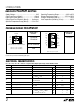
TRUTH TABLE
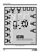
FREQUENCY (MHz)
1
–1
GAIN (dB)
PHASE (DEG)
0
1
2
3
10 100 1000
LT1203/05 • TPC02
–2
–3
–4
–5
4
5
–120
–100
–80
–60
–40
–140
–160
–180
–200
–20
0
V
S
= ±15V
T
A
= 25°C
R
L
=
∞
FREQUENCY (MHz)
1
–1
GAIN (dB)
PHASE (DEG)
0
1
2
3
10 100 1000
LT1203/05 • TPC01
–2
–3
–4
–5
4
5
–120
–100
–80
–60
–40
–140
–160
–180
–200
–20
0
V
S
= ±5V
T
A
= 25°C
R
L
=
∞
±5V Frequency Response ±15V Frequency Response