
Datasheet


7
LT1203/LT1205
TYPICAL PERFOR A CE CHARACTERISTICS
WU
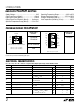
Channel 1 Disable
V
S
= ±15V
R
L
= 1k
LT1203/05 • TPC19
V
S
= ±15V
R
L
= 1k
Channel 1 Enable
LT1203/05 • TPC20
Input Protection
The logic inputs have ESD protection (≥2kV) and short-
ing them to 12V or 15V will cause excessive current to
flow. Limit the current to less than 50mA when driving
the logic above 6V. The analog inputs are protected
against ESD and overvoltage with internal SCRs. For
inputs ≥±2.8V the SCRs will fire and the DC current
should be limited to 20mA.
Power Supplies
The LT1203/LT1205 will operate from ±5V (10V total) to
±15V (30V total) and is specified over this range. Charac-
teristics change very little over this voltage range. It is not
necessary to use equal value supplies however, the output
offset voltage will change. The offset will change about
300µV per volt of supply mismatch. The LT1203/LT1205
have a very wide bandwidth yet are tolerant of power
supply bypassing. The power supplies should be by-
passed with a 0.1µF or 0.01µF ceramic capacitor within 0.5
inch of the part.
Circuit Layout
Use a ground plane to ensure a low impedance ground is
available throughout the PCB layout. Separate the inputs
U
S
A
O
PP
L
IC
AT
I
WU
U
I FOR ATIO
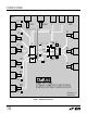
LT1203 Channel-to-Channel Switching Transient
with ground plane to ensure high channel separation. For
minimum peaking, maximum bandwidth and maximum
gain flatness sockets are not recommended because they
can add considerable stray inductance and capacitance. If
a socket must be used, use a low profile, low capacitance
socket such as the SamTec ISO-308.
Switching Transients
The LT1203/LT1205 use input buffers to ensure switching
transients do not couple to other video equipment sharing
the input line. Output switching transients are about
50mV
P-P
with a 20ns duration and input transients are
OUTPUT
50mV/DIV
INPUT
20mV/DIV
LOGIC
(PIN 5)
R
S
= 50Ω
LT1203/05 • AI01
V
INO
= 1V
V
IN1
= 0V
V
INO
= 1V
V
IN1
= 0V
EN
(PIN 6)
V
OUT
(PIN 7)
V
OUT
(PIN 7)
EN
(PIN 6)