
Datasheet


LT1206
9
1206fa
APPLICATIONS INFORMATION
is fl at to 0.35dB to 30MHz. The network has the greatest
effect for C
L
in the range of 0pF to 1000pF. The graph of
Maximum Capacitive Load vs Feedback Resistor can be
used to select the appropriate value of feedback resistor.
The values shown are for 0.5dB and 5dB peaking at a gain
of 2 with no resistive load. This is a worst case condition,
as the amplifi er is more stable at higher gains and with
some resistive load in parallel with the capacitance. Also
shown is the – 3dB bandwidth with the suggested feedback
resistor vs the load capacitance.
Although the optional compensation works well with ca-
pacitive loads, it simply reduces the bandwidth when it is
connected with resistive loads. For instance, with a 30Ω
load, the bandwidth drops from 55MHz to 35MHz when the
compensation is connected. Hence, the compensation was
made optional. To disconnect the optional compensation,
leave the COMP pin open.
Shutdown/Current Set
If the shutdown feature is not used, the SHUTDOWN pin
must be connected to ground or V
–
.
The shutdown pin can be used to either turn off the bias-
ing for the amplifi er, reducing the quiescent current to
less than 200µA, or to control the quiescent current in
normal operation.
The total bias current in the LT1206 is controlled by the cur-
rent fl owing out of the shutdown pin. When the shutdown
pin is open or driven to the positive supply, the part is shut
down. In the shutdown mode, the output looks like a 40pF
capacitor and the supply current is typically 100µA. The
shutdown pin is referenced to the positive supply through
an internal bias circuit (see the simplifi ed schematic). An
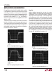
easy way to force shutdown is to use open drain (collec-
tor) logic. The circuit shown in Figure 2 uses a 74C904
buffer to interface between 5V logic and the LT1206. The
switching time between the active and shutdown states
is less than 1µs.
A 24k pull-up resistor speeds up the
turn-off time and insures that the LT1206 is completely
turned off. Because the pin is referenced to the positive
supply, the logic used should have a breakdown voltage
of greater than the positive supply voltage. No other
circuitry is necessary as the internal circuit limits the
shutdown pin current to about 500µA. Figure 3 shows
the resulting waveforms.
FREQUENCY (MHz)
1
–8
VOLTAGE GAIN (dB)
–4
0
4
8
10 100
LT1206 • F01
–6
–2
2
6
10
12
V
S
= ±15V
R
F
= 1.2k
COMPENSATION
R
F
= 2k
NO COMPENSATION
R
F
= 2k
COMPENSATION
Figure 1
–
+
LT1206
S/D
15V
–15V
R
F
R
G
V
IN
5V
24k
ENABLE
V
OUT
LT1206 • F02
15V
74C906
V
OUT
ENABLE
A
V
= 1
R
F
= 825Ω
R
L
= 50Ω
R
PU
= 24k
V
IN
= 1V
P-P
1µs/DIV
1206 F03
Figure 2. Shutdown Interface
Figure 3. Shutdown Operation