
Datasheet

14
LT1213/LT1214
U
S
A
O
PP
L
IC
AT
I
WU
U
I FOR ATIO
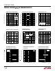
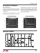
positive rail, is about 100Ω as the output starts to source
current; this resistance drops to about 20Ω as the current
increases. Therefore when the output sources 1mA, the
output will swing to within 0.7V of the positive supply.
While sourcing 30mA, it is within 1.25V of the positive
supply.
The output of the LT1213/LT1214 will swing to within 4mV
of the negative supply while sinking zero current. Thus, in
a typical single supply application with the load going to
ground, the output will go to within 4mV of ground. The
open-loop output resistance when the output is driven
hard into the negative rail is about 29Ω at low currents and
reduces to about 23Ω at high currents. Therefore when
the output sinks 1mA, the output is about 33mV above the
negative supply and while sinking 30mA, it is about
690mV above it.
The output of the LT1213/LT1214 has reverse-biased
diodes to each supply. If the output is forced beyond either
supply, unlimited currents will flow. If the current is
transient and limited to several hundred mA, no damage
will occur.
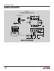
Feedback Components
Because the input currents of the LT1213/LT1214 are less
than 200nA, it is possible to use high value feedback
resistors to set the gain. However, care must be taken to
insure that the pole that is formed by the feedback resis-
tors and the input capacitance does not degrade the
stability of the amplifier. For example, if a single supply,
noninverting gain of two is set with two 10k resistors, the
LT1213/LT1214 will probably oscillate. This is because
the amplifier goes open-loop at 6MHz (6dB of gain) and
has 45° of phase margin. The feedback resistors and the
10pF input capacitance generate a pole at 3MHz that
introduces 63° of phase shift at 6MHz! The solution is
simple, lower the values of the resistors or add a feedback
capacitor of 10pF or more.
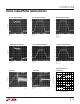
Inputs
Typically at room temperature, the inputs of the LT1213/
LT1214 can common mode 400mV below ground (V
–
)
and to within 1.2V of the positive supply with the amplifier
still functional. However, the input bias current and offset
voltage will shift as shown in the characteristic curves. For
full precision performance, the common mode range
should be limited between ground (V
–
) and 1.5V below the
positive supply.
When either of the inputs is taken below ground (V
–
) by
more than about 700mV, that input current will increase
dramatically. The current is limited by internal 100Ω
resistors between the input pins and diodes to each
supply. The output will remain low (no phase reversal) for
inputs 1.3V below ground (V
–
). If the output does not have
to sink current, such as in a single supply system with a 1k
load to ground, there is no phase reversal for inputs up to
8V below ground.
There are no clamps across the inputs of the LT1213/
LT1214 and therefore each input can be forced to any
voltage between the supplies. The input current will re-
main constant at about 100nA over most of this range.
When an input gets closer than 1.5V to the positive supply,
that input current will gradually decrease to zero until the
input goes above the supply, then it will increase due to the
previously mentioned diodes. If the inverting input is held
more positive than the noninverting input by 200mV or
more, while at the same time the noninverting input is
within 300mV of ground (V
–
), then the supply current will
increase by 2mA and the noninverting input current will
increase to about 10µA. This should be kept in mind in
comparator applications where the inverting input stays
above ground (V
–
) and the noninverting input is at or near
ground (V
–
).
Output
The output of the LT1213/LT1214 will swing to within
0.61V of the positive supply with no load. The open-loop
output resistance, when the output is driven hard into the