
Datasheet


8
LT1215/LT1216
Note 1: Absolute Maximum Ratings are those values beyond which the life
of a device may be impaired.
Note 2: A heat sink may be required to keep the junction temperature
below absolute maximum when the output is shorted indefinitely.
Note 3: The LT1215C/LT1216C are guaranteed functional over the
operating temperature range of –40°C to 85°C. The LT1215M is
guaranteed functional over the operating temperature range of
–55°C to 125°C.
Note 4: The LT1215C/LT1216C are guaranteed to meet specified
performance from 0°C to 70°C. The LT1215C/LT1216C are designed,
characterized and expected to meet specified performance from –40°C to
85°C but are not tested or QA sampled at these temperatures. For
guaranteed I-grade parts consult the factory. The LT1215M is guaranteed
to meet specified performance from –55°C to 125°C.
Note 5: T
J
is calculated from the ambient temperature T
A
and power
dissipation P
D
according to the following formulas:
LT1215MJ8, LT1215AMJ8: T
J
= T
A
+ (P
D
• 100°C/W)
LT1215CN8, LT1215ACN8: T
J
= T
A
+ (P
D
• 100°C/W)
LT1215CS8: T
J
= T
A
+ (P
D
• 150°C/W)
LT1216CN: T
J
= T
A
+ (P
D
• 70°C/W)
LT1216CS: T
J
= T
A
+ (P
D
• 100°C/W)
Note 6: This parameter is not 100% tested.
Note 7: Guaranteed by correlation to 3.3V and ±15V tests.
Note 8: Slew rate is measured between ±8.5V on an output swing of ±10V
on ±15V supplies.
Note 9: Most LT1215/LT1216 electrical characteristics change very little
with supply voltage. See the 5V tables for characteristics not listed in the
3.3V table.
Note 10: Guaranteed by correlation to 5V and ±15V tests.
Note 11: Guaranteed by correlation to 3.3V tests.
CCHARA TERIST
ICS
UW
AT
Y
P
I
CA
LPER
F
O
R
C
E
E
LECTR
IC
AL C CHARA TERIST
ICS
INPUT OFFSET VOLTAGE (µV)
–525
PERCENT OF UNITS (%)
50
45
40
35
30
25
20
15
10
5
0
–225
75
225
1215/16 G04
–375
–75
375
525
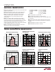
LT1215 N8 PACKAGE
LT1215 J8 PACKAGE
V
S
= 5V
Distribution of Offset Voltage Drift
Distribution of Input Offset Voltage with Temperature Distribution of Input Offset Voltage
OFFSET VOLTAGE DRIFT WITH TEMPERATURE (µV/°C)
–10
PERCENT OF UNITS (%)
50
40
30
20
10
0
6
1215/16 G08
–6
–2
2
10
LT1215 S8 PACKAGE
LT1216 N PACKAGE
LT1216 S PACKAGE
V
S
= 5V
–8
–4 0 4
8
INPUT OFFSET VOLTAGE (µV)
–750
PERCENT OF UNITS (%)
30
25
20
15
10
5
0
–450 –150 150 450
750
1215/16 G09
LT1215 S8 PACKAGE
LT1216 N PACKAGE
LT1216 S PACKAGE
V
S
= ±15V
INPUT OFFSET VOLTAGE (µV)
–525
PERCENT OF UNITS (%)
50
45
40
35
30
25
20
15
10
5
0
–225
75
225
1215/16 G07
–375
–75
375
525
LT1215 S8 PACKAGE
LT1216 N PACKAGE
LT1216 S PACKAGE
V
S
= 5V
OFFSET VOLTAGE DRIFT WITH TEMPERATURE (µV/°C)
–5
PERCENT OF UNITS (%)
50
40
30
20
10
0
3
1215/16 G05
–3
–1
1
5
LT1215 N8 PACKAGE
LT1215 J8 PACKAGE
V
S
= 5V
–4
–2 0 2
4
INPUT OFFSET VOLTAGE (µV)
–750
PERCENT OF UNITS (%)
30
25
20
15
10
5
0
–450 –150 150 450
750
1215/16 G06
LT1215 N8 PACKAGE
LT1215 J8 PACKAGE
V
S
= ±15V
Distribution of Offset Voltage Drift Distribution of Input Offset
Distribution of Input Offset Voltage with Temperature Voltage