
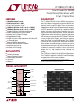
Datasheet

5
LT1280A/LT1281A
CCHARA TERIST
ICS
UW
AT
Y
P
I
CA
LPER
F
O
R
C
E
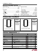
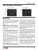
Shutdown to Driver Outputs
Driver Output Waveforms
LT1280A • TPC13
LT1280A • TPC12
PI FU CTIO S
U
UU
Output current capability is sufficient for load conditions
up to 2500pF. Outputs are in a high impedance state when
in shutdown mode or V
CC
= 0V. Outputs are fully short-
circuit protected from V
–
+ 30V to V
+
– 30V. Applying
higher voltages will not damage the device if the overdrive
is moderately current limited. Short circuits on one
output can load the power supply generator and may
disrupt the signal levels of the other outputs. The driver
outputs are protected against ESD to ±10kV for human
body model discharges.
REC1 IN, REC2 IN: Receiver Inputs. These pins accept
RS232 level signals (±30V) into a protected 5k terminat-
ing resistor. The receiver inputs are protected against ESD
to ±10kV for human body model discharges. Each receiver
provides 0.4V of hysteresis for noise immunity. Open
receiver inputs assume a logic low state.
REC1 OUT, REC2 OUT: Receiver outputs with TTL/CMOS
Voltage Levels. Outputs are in a high impedance state
when in shutdown mode to allow data line sharing. Out-
puts are fully short-circuit protected to ground or V
CC
with
the power ON, OFF or in the shutdown mode.
C1
+
, C1
–
, C2
+
, C2
–
: Commutating Capacitor Inputs.
These pins require two external capacitors C ≥ 0.1µF: one
from C1
+
to C1
–
and another from C2
+
to C2
–
. C1 should
be deleted if a separate 12V supply is available and
connected to pin C1
+
. Similarly, C2 should be deleted if a
separate –12V supply is connected to pin V
–
.
INPUT
DRIVER OUTPUT
R
L
= 3k
DRIVER OUTPUT
R
L
= 3k
C
L
= 2500pF
10V
5V
GND
DRIVER 1
OUTPUT
DRIVER 2
OUTPUT
ON/OFF PIN
GND
–10V
–5V
V
CC
: 5V Input Supply Pin. This pin should be decoupled
with a 0.1µF ceramic capacitor close to the package pin.
Insufficient supply bypassing can result in low output
drive levels and erratic charge pump operation.
GND: Ground Pin.
ON/OFF: A TTL/CMOS Compatible Operating Mode Con-
trol. A logic low puts the LT1280A in shutdown mode.
Supply current drops to zero and both driver and receiver
outputs assume a high impedance state. A logic high fully
enables the device.
V
+
: Positive Supply Output (RS232 Drivers). V
+
≈ 2V
CC
–
1.5V. This pin requires an external charge storage capaci-
tor C ≥ 0.1µF, tied to ground or V
CC
. Larger value capaci-
tors may be used to reduce supply ripple. With multiple
transceivers, the V
+
and V
–
pins may be paralleled into
common capacitors.
V
–
: Negative Supply Output (RS232 Drivers). V
–
≈ –
(2V
CC
– 2.5V). This pin requires an external charge storage
capacitor C ≥ 0.1µF. Larger value capacitors may be used
to reduce supply ripple. With multiple transceivers, the V
+
and V
–
pins may be paralleled into common capacitors.
TR1 IN, TR2 IN: RS232 Driver Input Pins. These inputs are
TTL/CMOS compatible. Inputs should not be allowed to
float. Tie unused inputs to V
CC
.
TR1 OUT, TR2 OUT: Driver Outputs at RS232 Voltage
Levels. Driver output swing meets RS232 levels for loads
up to 3k. Slew rates are controlled for lightly loaded lines.