
Datasheet


LT1366/LT1367
LT1368/LT1369
12
1366fb
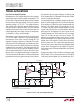
Technology’s proprietary complementary bipolar process,
which ensures very similar DC and AC characteristics for
the output devices Q24 and Q26.
A simple comparator Q5 steers current from current source
I
1
between the two input stages. When the input common
mode voltage V
CM
is near the negative supply, Q5 is re-
verse biased, and I
1
becomes the tail current for the PNP
differential pair Q1/Q2. At the other extreme, when V
CM
is within about 1.3V from the positive supply, Q5 diverts
I
1
to the current mirror D3/Q6, which furnishes the tail
current for the NPN differential pair Q3/Q4.
The collector currents of the two input pairs are combined
in the second stage, consisting of Q7 through Q11. Most
of the voltage gain in the amplifier is contained in this
stage. Differential amplifier Q14/Q15 buffers the output
of the second stage, converting the output voltage to dif-
ferential currents. The differential currents pass through
current mirrors D4/Q17 and D5/Q16, and are converted to
differential voltages by Q18 and Q19. These voltages are
also buffered and applied to the output Darlington pairs
Q23/Q24 and Q25/Q26. Capacitors C1 and C2 form local
feedback loops around the output devices, lowering the
output impedance at high frequencies.
Input Offset Voltage
Since the amplifier has two input stages, the input offset
voltage changes depending upon which stage is active.
The input offsets are random, but bounded voltages. When
the amplifier switches between stages, offset voltages
may go up, down, or remain flat; but will not exceed the
guaranteed limits. This behavior is illustrated in three
distribution plots of input offset voltage in the Typical
Performance Characteristics section.
Overdrive Protection
Two circuits prevent the output from reversing polarity
when the input voltage exceeds the common mode range.
When the noninverting input exceeds the positive supply
by approximately 300mV, the clamp transistor Q12 (Fig-
ure
1) turns on, pulling the output of the second stage
low, which forces the output high. For inputs below the
negative supply, diodes D1 and D2 turn on, overcoming
the saturation of the input pair Q1/Q2.
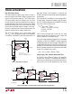
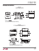
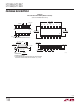
When overdriven, the amplifier draws input current that
exceeds the normal input bias current. Figures 2 and 3
show some typical overdrive currents as a function of
input voltage. The input current must be less than 1mA of
positive overdrive or less than 7mA of negative overdrive,
for the phase reversal protection to work properly. When
the amplifier is severely overdriven, an external resistor
should be used to limit the overdrive current. In addition
to overdrive protection, the amplifier is protected against
ESD strokes up to 4kV on all pins.
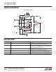
applicaTions inForMaTion
COMMON MODE VOLTAGE RELATIVE TO
POSITIVE SUPPLY (mV)
–500
0
INPUT BIAS CURRENT (nA)
20
40
60
80
–300 –100 V
S
LT1366 F02
100
100
110
90
70
50
30
10
300 500
T = –55°C
T = 25°C
T = 85°C
T = 70°C
MEASURED AS A
FOLLOWER
–
+
Figure 2. Input Bias Current vs Common Mode Voltage
COMMON MODE VOLTAGE RELATIVE TO
NEGATIVE SUPPLY (mV)
–800
–110
INPUT BIAS CURRENT (nA)
–90
–70
–50
–30
–600 –400
LT1366 F03
–200
–10
0
–20
–40
–60
–80
–100
V
S
200
T = –55°C T = 25°C
T = 85°C
–
+
T = 70°C
MEASURED AS A FOLLOWER
Figure 3. Input Bias Current vs Common Mode Voltage