
Datasheet


15
LT1374
1374fd
APPLICATIONS INFORMATION
WUU
U
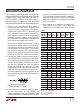
Threshold voltage for lockout is about 2.38V, slightly less
than the internal 2.42V reference voltage. A 3.5µA bias
current flows
out
of the pin at threshold. This internally
generated current is used to force a default high state on
the shutdown pin if the pin is left open. When low shut-
down current is not an issue, the error due to this current
can be minimized by making R
LO
10k or less. If shutdown
current is an issue, R
LO
can be raised to 100k, but the error
due to initial bias current and changes with temperature
should be considered.
V
IN
= Minimum input voltage
Keep the connections from the resistors to the shutdown
pin short and make sure that interplane or surface capaci-
tance to the switching nodes are minimized. If high
resistor values are used, the shutdown pin should be
bypassed with a 1000pF capacitor to prevent coupling
problems from the switch node. If hysteresis is desired in
the undervoltage lockout point, a resistor R
FB
can be
added to the output node. Resistor values can be calcu-
lated from:
25k suggested for R
LO
V
IN
=
Input voltage at which switching stops as input
voltage descends to trip level
∆V = Hysteresis in input voltage level
Example: output voltage is 5V, switching is to stop if input
voltage drops below 12V and should not restart unless
input rises back to 13.5V. ∆V is therefore 1.5V and
V
IN
= 12V. Let R
LO
= 25k.
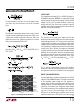
SWITCH NODE CONSIDERATIONS
For maximum efficiency, switch rise and fall times are
made as short as possible. To prevent radiation and high
frequency resonance problems, proper layout of the com-
ponents connected to the switch node is essential. B field
(magnetic) radiation is minimized by keeping catch diode,
switch pin, and input bypass capacitor leads as short as
possible. E field radiation is kept low by minimizing the
length and area of all traces connected to the switch pin
and BOOST pin. A ground plane should always be used
under the switcher circuitry to prevent interplane cou-
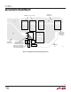
pling. A suggested layout for the critical components is
shown in Figure 5. Note that the feedback resistors and
compensation components are kept as far as possible
from the switch node. Also note that the high current
ground path of the catch diode and input capacitor are kept
very short and separate from the analog ground line.
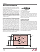
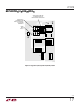
The high speed switching current path is shown schemati-
cally in Figure 6. Minimum lead length in this path is
essential to ensure clean switching and low EMI. The path
including the switch, catch diode, and input capacitor is
the only one containing nanosecond rise and fall times. If
you follow this path on the PC layout, you will see that it is
irreducibly short. If you move the diode or input capacitor
away from the LT1374, get your resumé in order. The
other paths contain only some combination of DC and
500kHz triwave, so are much less critical.