
Datasheet

18
LT1375/LT1376
13756fd
APPLICATIONS INFORMATION
WUU
U
practice therefore to simply use the worst-case value and
assume that RMS ripple current is one half of load current.
At maximum output current of 1.5A for the LT1376, the
input bypass capacitor should be rated at 0.75A ripple
current. Note however, that there are many secondary
considerations in choosing the final ripple current rating.
These include ambient temperature, average versus peak
load current, equipment operating schedule, and required
product lifetime. For more details, see Application Notes
19 and 46, and Design Note 95.
Input Capacitor Type
Some caution must be used when selecting the type of
capacitor used at the input to regulators. Aluminum
electrolytics are lowest cost, but are physically large to
achieve adequate ripple current rating, and size con-
straints (especially height), may preclude their use. Ce-
ramic capacitors are now available in larger values, and
their high ripple current and voltage rating make them
ideal for input bypassing. Cost is fairly high and footprint
may also be somewhat large. Solid tantalum capacitors
would be a good choice, except that they have a history of
occasional spectacular failures when they are subjected to
large current surges during power-up. The capacitors can
short and then burn with a brilliant white light and lots of
nasty smoke. This phenomenon occurs in only a small
percentage of units, but it has led some OEM companies
to forbid their use in high surge applications. The input
bypass capacitor of regulators can see these high surges
when a battery or high capacitance source is connected.
Several manufacturers have developed a line of solid
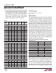
tantalum capacitors specially tested for surge capability
(AVX TPS series for instance, see Table 3), but even these
units may fail if the input voltage surge approaches the
maximum voltage rating of the capacitor. AVX recom-
mends derating capacitor voltage by 2:1 for high surge
applications. The highest voltage rating is 50V, so 25V
may be a practical upper limit when using solid tantalum
capacitors for input bypassing.
Larger capacitors may be necessary when the input volt-
age is very close to the minimum specified on the data
sheet. Small voltage dips during switch on time are not
normally a problem, but at very low input voltage they may
cause erratic operation because the input voltage drops
below the minimum specification. Problems can also
occur if the input-to-output voltage differential is near
minimum. The amplitude of these dips is normally a
function of capacitor ESR and ESL because the capacitive
reactance is small compared to these terms. ESR tends to
be the dominate term and is inversely related to physical
capacitor size within a given capacitor type.
Minimum Input Voltage (After Start-Up)
Minimum input voltage to make the LT1376 “run” cor-
rectly is typically 5V, but to regulate the output, a buck
converter input voltage must always be higher than the
output voltage. To calculate minimum operating input
voltage, switch voltage loss and maximum duty cycle
must be taken into account. With the LT1376, there is the
additional consideration of proper operation of the boost
circuit. The boost circuit allows the power switch to
saturate for high efficiency, but it also sometimes results
in a start-up or operating voltage that is several volts
higher than the standard running voltage, especially at
light loads. An approximate formula to calculate minimum
running
voltage at load currents above 100mA is:
V
VI
IN MIN
OUT OUT
(
)
=
+
()( )
04
088
.
.
Ω
Minimum Start-Up Voltage and Operation at
Light Loads
The boost capacitor supplies current to the BOOST pin
during switch on time. This capacitor is recharged only
during switch off time. Under certain conditions of light
load and low input voltage, the capacitor may not be
recharged fully during the relatively short off time. This
causes the boost voltage to collapse and minimum input
voltage is increased. Start-up voltage at light loads is
higher than normal running voltage for the same reasons.
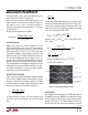
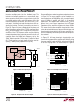
The graph in Figure 9 shows minimum input voltage for a
5V output, both for start-up and for normal operation.
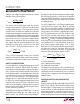
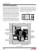
The circuit in Figure 10 will allow operation at light load
with low input voltages. It uses a small PNP to charge the
boost capacitor C2, and an extra diode D3 to complete the
power path from V
SW
to the boost capacitor.