
Datasheet


1
LT1381
Low Power 5V RS232 Dual
Driver/Receiver with
0.1µF Capacitors
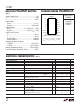
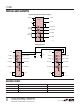
R
Output Waveforms
DRIVER
OUTPUT
R
L
= 3k
C
L
= 2500pF
RECEIVER
OUTPUT
C
L
= 50pF
INPUT
U
S
A
O
PP
L
IC
AT
I
■
Portable Computers
■
Battery-Powered Systems
■
Power Supply Generator
■
Terminals
■
Modems
U
A
O
PP
L
IC
AT
ITY
P
I
CA
L
D
U
ESCRIPTIO
S
F
EA
T
U
RE
■
ESD Protection over ±10kV
■
Low Cost
■
Uses Small Capacitors: 0.1µF
■
CMOS Comparable Low Power: 40mW
■
Operates from a Single 5V Supply
■
120kBaud Operation for R
L
= 3k, C
L
= 2500pF
■
250kBaud Operation for R
L
= 3k, C
L
= 1000pF
■
Rugged Bipolar Design
■
Outputs Assume a High Impedance State When
Powered Down
■
Absolutely No Latchup
■
Available in Narrow SO Package
5k
5k
0.1µF
LOGIC
INPUTS
LOGIC
OUTPUTS
9
12
10
11
5
4
3
1
15
8
13
7
14
6
2
16
5V INPUT
V
+
OUT
V
–
OUT
RS232 OUTPUT
RS232 OUTPUT
RS232 INPUT
RS232 INPUT
LT1381 • TA01
LT1381
0.1µF
0.1µF
0.1µF
+
+
+
+
S
, LTC and LT are registered trademarks of Linear Technology Corporation.
TransZorb
®
is a registered trademark of General Instruments, GSI
The LT
®
1381 is a dual RS232 driver/receiver pair with
integral charge pump to generate RS232 voltage levels
from a single 5V supply. The circuit features rugged
bipolar design to provide operating fault tolerance and
ESD protection unmatched by competing CMOS designs.
Using only 0.1µF external capacitors, the circuit con-
sumes only 40mW of power and can operate to 120kbaud
even while driving heavy capacitive loads. New ESD struc-
tures on the chip allow the LT1381 to survive multiple
±10kV strikes, eliminating the need for costly TransZorbs
®
on the RS232 line pins. Driver outputs are protected from
overload and can be shorted to ground or up to ±25V
without damage. During power-off conditions, driver and
receiver outputs are in a high impedance state, allowing
line sharing.
LT1381 • TA02