
Datasheet


3
LT1381
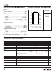
PARAMETER CONDITIONS MIN TYP MAX UNITS
Receiver
Input Voltage Thresholds Input Low Threshold (V
OUT
= High) 0.8 1.3 V
Input High Threshold (V
OUT
= Low) 1.7 2.4 V
Hysteresis ● 0.1 0.4 1.0 V
Input Resistance (Note 6) 3 5 7 kΩ
Output Voltage Output Low, I
OUT
= –1.6mA ● 0.2 0.4 V
Output High, I
OUT
= 160µA (V
CC
= 5V) ● 3.5 4.2 V
Output Short-Circuit Current Sinking Current, V
OUT
= V
CC
–10 mA
Sourcing Current, V
OUT
= 0V 10 20 mA
Propagation Delay Output Transition t
HL
High-to-Low (Note 5) 250 600 ns
Output Transition t
LH
Low-to-High 350 600 ns
E
LECTR
IC
AL C CHARA TERIST
ICS
(Note 2)
TYPICAL PERFOR A CE CHARACTERISTICS
WU
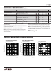
Driver Maximum Output Voltage
vs Load Capacitance
TEMPERATURE (°C)
–55
–10
DRIVER OUTPUT VOLTAGE (V)
–8
–4
–2
0
10
4
0
50
75
LT1381 • TPC03
–6
6
8
2
–25
25
100
125
R
L
= 3k
V
CC
= 5.5V
V
CC
= 5V
V
CC
= 4.5V
V
CC
= 4.5V
V
CC
= 5V
V
CC
= 5.5V
OUTPUT HIGH
OUTPUT LOW
Driver Minimum Output Voltage
vs Load Capacitance Driver Output Voltage
Note 4: For driver delay measurements, R
L
= 3k and C
L
= 51pF. Trigger
points are set between the driver’s input logic threshold and the output
transition to the zero crossing (t
HL
= 1.4V to 0V and t
LH
= 1.4V to 0V).
Note 5: For receiver delay measurements, C
L
= 51pF. Trigger points are
set between the receiver’s input logic threshold and the output transition
to standard TTL/CMOS logic threshold (t
HL
= 1.3V to 2.4V and t
LH
= 1.7V
to 0.8V).
Note 6: Tested at V
IN
= ±10V.
The ● denotes specifications which apply over the full operating
temperature range.
Note 1: Absolute Maximum Ratings are those values beyond which the life
of the device may be impaired.
Note 2: Testing done at V
CC
= 5V, unless otherwise specified.
Note 3: Supply current is measured as the average over several charge
pump cycles. C
+
= C
–
= C1 = C2 = 0.1µF. All outputs are open, with all
driver inputs tied high.
–20
LOAD CAPACITANCE (nF)
–7.0
PEAK OUTPUT VOLTAGE (V)
–6.0
–5.0
–4.0
2468
LT1381 • TPC02
1013579
–5.5
–4.5
–6.5
0
2 DRIVERS LOADED
120k BAUD
60k BAUD
20k BAUD
LOAD CAPACITANCE (nF)
0
PEAK OUTPUT VOLTAGE (V)
8.0
9.0
8
LT1381 • TPC01
7.0
6.0
5.0
2
4
6
10
7.5
8.5
6.5
5.5
7
1
3
5
9
2 DRIVERS LOADED
20k BAUD
60k BAUD
120k BAUD