
Datasheet


LT1460
19
1460fc
Input Capacitance
It is recommended that a 0.1µF or larger capacitor be
added to the input pin of the LT1460. This can help with
stability when large load currents are demanded.
Output Accuracy
Like all references, either series or shunt, the error budget of
the LT1460-2.5 is made up of primarily three components:
initial accuracy, temperature coefficient and load regulation.
Line regulation is neglected because it typically contrib-
utes only 30ppm/V, or 75µV for a 1V input change. The
LT1460-2.5 typically shifts less than 0.01% when soldered
into a PCB, so this is also neglected (see PC Board Layout
section). The output errors are calculated as follows for a
100µA load and 0°C to 70°C temperature range:
LT1460AC
Initial accuracy = 0.075%
For I
O
= 100µA, and using the LT1460-2.5 for calculation,
ΔV
ppm
mA
mA V V
OUT
=
( )( )
=
3500
0 1 2 5 875. . µ
which is 0.035%.
For temperature 0°C to 70°C the maximum ΔT = 70°C,
ΔV
ppm
C
C V mV
OUT
=
°
°
( )( )
=
10
70 2 5 1 75. .
which is 0.07%.
Total worst-case output error is:
0.075% + 0.035% + 0.070% = 0.180%.
Table 1 gives worst-case accuracy for the LT1460AC, CC,
DC, FC, GC from 0°C to 70°C and the LT1460BI, EI, GI
from –40°C to 85°C.
Note that the LT1460-5 and LT1460-10 give identical ac-
curacy as a fraction of their respective output voltages.
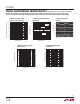
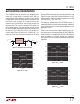
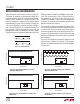
PC Board Layout
In 13- to 16-bit systems where initial accuracy and tem-
perature coefficient calibrations have been done, the me-
chanical and thermal stress on a PC board (in a cardcage
for instance) can shift the output voltage and mask the
true temperature coefficient of a reference. In addition,
the mechanical stress of being soldered into a PC board
can cause the output voltage to shift from its ideal value.
Surface mount voltage references (MS8 and S8) are the
most susceptible to PC board stress because of the small
amount of plastic used to hold the lead frame.
A simple way to improve the stress-related shifts is to
mount the reference near the short edge of the PC board,
or in a corner. The board edge acts as a stress boundary,
or a region where the flexure of the board is minimum.
The package should always be mounted so that the leads
absorb the stress and not the package. The package is
generally aligned with the leads parallel to the long side
of the PC board as shown in Figure 20a.
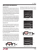
A qualitative technique to evaluate the effect of stress on
voltage references is to solder the part into a PC board and
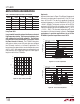
Table 2. Worst-Case Output Accuracy Over Temperature
I
OUT
LT1460AC LT1460BI LT1460CC LT1460DC LT1460EI LT1460FC LT1460GC LT1460GI LT1460HC LT1460JC LT1460KC
0 0.145% 0.225% 0.205% 0.240% 0.375% 0.325% 0.425% 0.562% 0.340% 0.540% 0.850%
100µA 0.180% 0.260% 0.240% 0.275% 0.410% 0.360% 0.460% 0.597% 0.380% 0.580% 0.890%
10mA 0.325% 0.405% 0.385% 0.420% 0.555% 0.505% 0.605% 0.742% 0.640% 0.840% 1.15%
20mA 0.425% N/A 0.485% 0.520% N/A 0.605% 0.705% N/A 0.540% 0.740% 1.05%
applications inForMation