
Datasheet


LT1460
7
1460fc
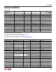
PARAMETER CONDITIONS MIN TYP MAX UNITS
Output Voltage Noise (Note 7)
LT1460A, LT1460B, LT1460C, LT1460D, LT1460E,
LT1460F, LT1460G, LT1460H, LT1460L, LT1460M
LT1460-2.5
0.1Hz ≤ f ≤ 10Hz
10Hz ≤ f ≤ 1kHz
10
10
µV
P-P
µV
RMS
LT1460-5 0.1Hz ≤ f ≤ 10Hz
10Hz ≤ f ≤ 1kHz
20
20
µV
P-P
µV
RMS
LT1460-10 0.1Hz ≤ f ≤ 10Hz
10Hz ≤ f ≤ 1kHz
40
35
µV
P-P
µV
RMS
LT1460HC, LT1460JC, LT1460KC 0.1Hz ≤ f ≤ 10Hz
10Hz ≤ f ≤ 1kHz
4
4
ppm (P-P)
ppm (RMS)
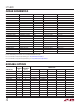
Long-Term Stability of Output Voltage (Note 8)
S8 Pkg
40 ppm/√kHr
LT1460HC, L
T1460JC, LT1460KC 100 ppm/√kHr
Hysteresis (Note 9)
LT1460A, LT1460B, LT1460C, LT1460D, LT1460E,
LT1460F, LT1460G, LT1460H, LT1460L, LT1460M
ΔT = 0°C to 70°C
ΔT = –40°C to 85°C
25
160
ppm
ppm
LT1460HC, L
T1460JC, LT1460KC
ΔT = 0°C to 70°C
ΔT = –40°C to 85°C
l
l
50
250
ppm
ppm
Note 1: Stresses beyond those listed under Absolute Maximum Ratings
may cause permanent damage to the device. Exposure to any Absolute
Maximum Rating condition for extended periods may affect device
reliability and lifetime.
Note 2: If the part is stored outside of the specified temperature range, the
output may shift due to hysteresis.
Note 3: Temperature coefficient is measured by dividing the change in
output voltage by the specified temperature range. Incremental slope is
also measured at 25°C.
Note 4: Load regulation is measured on a pulse basis from no load to the
specified load current. Output changes due to die temperature change
must be taken into account separately.
Note 5: Thermal regulation is caused by die temperature gradients created
by load current or input voltage changes. This effect must be added to
normal line or load regulation. This parameter is not 100% tested.
Note 6: Excludes load regulation errors. For LT1460S3, ΔV
OUT
≤ 0.2%. For
all other packages, ΔV
OUT
≤ 0.1%.
Note 7: Peak-to-peak noise is measured with a single highpass filter at
0.1Hz and 2-pole lowpass filter at 10Hz. The unit is enclosed in a still-air
environment to eliminate thermocouple effects on the leads. The test time
is 10 sec. RMS noise is measured with a single highpass filter at 10Hz and
a 2-pole lowpass filter at 1kHz. The resulting output is full wave rectified
The l denotes the specifications which apply over the full operating
temperature range, otherwise specifications are at T
A
= 25°C. V
IN
= V
OUT
+ 2.5V, I
OUT
= 0 unless otherwise specified.
and then integrated for a fixed period, making the final reading an average
as opposed to RMS. A correction factor of 1.1 is used to convert from
average to RMS and a second correction of 0.88 is used to correct for the
nonideal pass band of the filters.
Note 8: Long-term stability typically has a logarithmic characteristic and
therefore, changes after 1000 hours tend to be much smaller than before
that time. Total drift in the second thousand hours is normally less than
one third that of the first thousand hours with a continuing trend toward
reduced drift with time. Significant improvement in long-term drift can
be realized by preconditioning the IC with a 100 hour to 200 hour, 125°C
burn-in. Long-term stability will also be affected by differential stresses
between the IC and the board material created during board assembly. See
PC Board Layout in the Applications Information section.
Note 9: Hysteresis in output voltage is created by package stress that
differs depending on whether the IC was previously at a higher or lower
temperature. Output voltage is always measured at 25°C, but the IC is
cycled to 85°C or –40°C before successive measurements. Hysteresis
is roughly proportional to the square of the temperature change. For
instruments that are stored at reasonably well-controlled temperatures
(within 20 or 30 degrees of operating temperature) hysteresis is generally
not a problem.
Note 10: The LT1460S3 is guaranteed functional over the operating
temperature range of –40° to 85°C.
electrical characteristics