
Datasheet

22
LT1506
APPLICATIONS INFORMATION
WUU
U
converters 120° out of phase with each other reduces
input and output ripple currents. This reduces the ripple
rating, size and cost of filter capacitors.
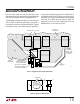
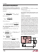
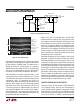
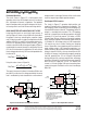
Current Sharing/Split Input Supplies
Current sharing is accomplished by joining the V
C
pins to
a common compensation capacitor. The output of the
error amplifier is a gm stage, so any number of devices can
be connected together. The effective gm of the composite
error amplifier is the multiple of the individual devices. In
Figure 15, the compensation capacitor C4 has been
increased by ×3. Tolerances in the reference voltages
result in small offset currents to flow between the V
C
pins.
The overall effect is that the loop regulates the output at a
voltage between the minimum and maximum reference of
the devices used. Switch current matching between
devices will be typically better than 300mA. The negative
temperature coefficient of the V
C
to switch current transcon-
ductance prevents current hogging.
A common V
C
voltage forces each LT1506 to operate at the
same switch current, not duty cycle. Each device operates
at the duty cycle defined by its respective input voltage. In
Figure 15, the input could be split and each device oper-
ated at a different voltage. The common V
C
ensures
loading is shared between inputs.
Figure 15. Current Sharing 12A Supply
+
+
C4
68nF
25V
C1, C3: MARCON THCS50E1E106Z
D1: ROHM RB051L-40
D2: 1N914
L1: DO3316P-682
+
C3C
10µF
25V
C2C
330nF
10V
D1C
D2C
1506 F15
L1C
6.8µH
+
C1
10µF
25V
5V
12A
R1
5.36k
1%
R2
4.99k
1%
1.8MHz
3-BIT RING
COUNTER
+
+
C3B
10µF
25V
C2B
330nF
10V
D1B
D2B
L1B
6.8µH
+
+
C3A
10µF
25V
INPUT
6V TO 15V
C2A
330nF
10V
D1A
D2A
L1A
6.8µH
V
C
SYNC SW GND
LT1506-SYNC
V
IN
BOOST FBV
C
SYNC SW GND
LT1506-SYNC
V
IN
BOOST FBV
C
SYNC SW GND
LT1506-SYNC
V
IN
BOOST FB
Synchronized Ripple Currents
A ring counter generates three synchronization signals at
600kHz, 33% duty cycle phased 120° apart. The sync
input will operate over a wide range of duty cycles, so no
further pulse conditioning is needed. Each device’s maxi-
mum input ripple current is a 4A square wave at 600kHz.
When synchronously added together, the ripple remains
at 4A but frequency increases to 1.8MHz. Likewise, the
output ripple current is a 1.8MHz triangular waveform,
with maximum amplitude of 350mA at 10V V
IN
. Interest-
ingly, at 7.6V and 15V V
IN
, the theoretical summed output
ripple current cancels completely. To reduce board space
and ripple voltage, C1 and C3 are ceramic capacitors. Loop
compensation C4 must be adjusted when using ceramic
output capacitors due to the lack of effective series resis-
tance. The typical tantalum compensation of 1.5nF is
increased to 22nF (×3) for the ceramic output capacitor.
If synchronization is not used and the internal oscillators
free run, the circuit will operate correctly, but ripple
cancellation will not occur. Input and output capacitors
must be ripple rated for the total output current.