
Datasheet


3
LT1513/LT1513-2
sn1513 1513fas
E
LECTR
IC
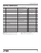
AL C CHARA TERIST
ICS
V
IN
= 5V, V
C
= 0.6V, V
FB
= V
REF
, I
FB
= 0V, V
SW
and S/S pins open, unless otherwise noted.
SYMBOL PARAMETER CONDITIONS MIN TYP MAX UNITS
Error Amplifier Clamp Voltage High Clamp, V
FB
= 1V 1.70 1.95 2.30 V
Low Clamp, V
FB
= 1.5V 0.25 0.40 0.52 V
A
V
Error Amplifier Voltage Gain 500 V/V
V
C
Pin Threshold Duty Cycle = 0% 0.8 1 1.25 V
f Switching Frequency 2.7V ≤ V
IN
≤ 25V 450 500 550 kHz
0°C ≤ T
J
≤ 125°C 430 500 580 kHz
T
J
< 0°C 400 580 kHz
Maximum Switch Duty Cycle ● 85 95 %
Switch Current Limit Blanking Time 130 260 ns
BV Output Switch Breakdown Voltage 0°C ≤ T
J
≤ 125°C4047V
T
J
< 0°C35V
V
SAT
Output Switch ON Resistance I
SW
= 2A ● 0.25 0.45 Ω
I
LIM
Switch Current Limit Duty Cycle = 50% ● 3.0 3.8 5.4 A
Duty Cycle = 80% (Note 1) ● 2.6 3.4 5.0 A
∆I
IN
/∆I
SW
Supply Current Increase During Switch ON Time 15 25 mA/A
Control Voltage to Switch Current 4A/V
Transconductance
Minimum Input Voltage ● 2.4 2.7 V
I
Q
Supply Current 2.7V ≤ V
IN
≤ 25V ● 4 5.5 mA
Shutdown Supply Current 2.7V ≤ V
IN
≤ 25V, V
S/S
≤ 0.6V, T
J
≥ 0°C ● 12 30 µA
T
J
< 0°C50µA
Shutdown Threshold 2.7V ≤ V
IN
≤ 25V ● 0.6 1.3 2 V
Shutdown Delay ● 51225µs
S/S Pin Input Current 0V ≤ V
S/S
≤ 5V ● –10 15 µA
Synchronization Frequency Range ● 600 800 kHz
The ● denotes specifications which apply over the full operating
temperature range.
Note 1: For duty cycles (DC) between 50% and 85%, minimum
guaranteed switch current is given by I
LIM
= 1.33 (2.75 – DC).
Note 2: The I
FB
pin is servoed to its regulating state with V
C
= 0.8V.
Note 3: Consult factory for grade selected parts.
Note 4: The I
FB
pin is sevoed to regulate FB to 1.245V