
Datasheet


8
LT1528
1528fa
The LT1528 is specified with the SENSE pin tied to the
OUTPUT pin. This sets the output voltage to 3.3V. Speci-
fications for output voltage greater than 3.3V will be
proportional to the ratio of the desired output voltage to
3.3V (V
OUT
/3.3V). For example, load regulation for an
output current change of 1mA to 1.5A is –5mV (typical) at
V
OUT
= 3.3V. At V
OUT
= 12V, load regulation would be:
(12V/3.3V) • (–5mV) = (–18mV)
Thermal Considerations
The power handling capability of the device will be limited
by the maximum rated junction temperature (125°C). The
power dissipated by the device will be made up of two
components:
1. Output current multiplied by the input/output voltage
differential, I
OUT
• (V
IN
– V
OUT
), and
2. GND pin current multiplied by the input voltage,
I
GND
• V
IN.
The GND pin current can be found by examining the GND
Pin Current curves in the Typical Performance Character-
istics. Power dissipation will be equal to the sum of the two
components listed above.
The LT1528 has internal thermal limiting designed to
protect the device during overload conditions. For
continuous normal load conditions the maximum junction
temperature rating of 125°C must not be exceeded. It is
important to give careful consideration to all sources of
thermal resistance from junction-to-ambient. Additional
heat sources mounted nearby must also be considered.
For surface mount devices heat sinking is accomplished
by using the heat spreading capabilities of the PC board
and its copper traces. Experiments have shown that the
heat spreading copper layer does not have to be electri-
cally connected to the tab of the device. The PC material
can be very effective at transmitting heat between the pad
area, attached to the tab of the device, and a ground or
power plane either inside or on the opposite side of the
board. Although the actual thermal resistance of the PC
material is high, the length/area ratio of the thermal
resistor between layers is small. Copper board stiffeners
and plated through holes can also be used to spread the
heat generated by power devices.
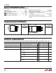
Table 1a lists thermal resistance for the DD package. For the
TO-220 package (Table 1b) thermal resistance is given for
junction-to-case only since this package is usually mounted
to a heat sink. Measured values of thermal resistance for
several different copper areas are listed for the DD package.
All measurements were taken in still air on 3/32" FR-4 board
with one ounce copper. This data can be used as a rough
guideline in estimating thermal resistance. The thermal
resistance for each application will be affected by thermal
interactions with other components as well as board size and
shape. Some experimentation will be necessary to determine
the actual value.
Table 1a. Q-Package, 5-Lead DD
COPPER AREA
THERMAL RESISTANCE
TOPSIDE* BACKSIDE BOARD AREA
(JUNCTION-TO-AMBIENT)
2500 sq mm 2500 sq mm 2500 sq mm 23°C/W
1000 sq mm 2500 sq mm 2500 sq mm 25°C/W
125 sq mm 2500 sq mm 2500 sq mm 33°C/W
*Device is mounted on topside.
Table 1b. T Package, 5-Lead TO-220
Thermal Resistance (Junction-to-Case) 2.5°C/W
Calculating Junction Temperature
Example: Given an output voltage of 3.3V, an input voltage
range of 4.5V to 5.5V, an output current range of 0mA to
500mA and a maximum ambient temperature of 50°C,
what will the maximum junction temperature be?
The power dissipated by the device will be equal to:
I
OUT(MAX)
• (V
IN(MAX)
– V
OUT
) + [I
GND
• V
IN(MAX)
]
where,
I
OUT(MAX)
= 500mA
V
IN(MAX)
= 5.5V
I
GND
at (I
OUT
= 500mA, V
IN
= 5.5V) = 4mA
so,
P = 500mA • (5.5V – 3.3V) + (4mA • 5.5V) = 1.12W
If we use a DD package, the thermal resistance will be in
the range of 23°C/W to 33°C/W depending on the copper
area. So the junction temperature rise above ambient will
be approximately equal to:
1.12W • 28°C/W = 31.4°C
APPLICATIO S I FOR ATIO
WUUU