
Datasheet


9
LT1528
1528fa
The maximum junction temperature will be equal to the
maximum junction temperature rise above ambient plus
the maximum ambient temperature or:
T
JMAX
= 50°C + 31.4°C = 81.4°C
Output Capacitance and Transient Performance
The LT1528 is designed to be stable with a wide range of
output capacitors. The minimum recommended value is
3.3µF with an ESR of 2Ω or less. The LT1528 output
transient response will be a function of output capaci-
tance. See the Transient Response curves in the Typical
Performance Characteristics. Larger values of output ca-
pacitance will decrease the peak deviations and provide
improved output transient response for larger load tran-
sients. Bypass capacitors, used to decouple individual
components powered by the LT1528, will increase the
effective value of the output capacitor.
Microprocessor Applications
The LT1528 has been optimized for microprocessor
applications, with the fastest transient response of current
PNP low dropout regulators. In order to deal with the large
load transients associated with current generation
microprocessors, output capacitance must be increased.
To meet worst-case voltage specifications for many popular
processors, four 47µF solid tantalum surface mount
capacitors are recommended for decoupling at the
microprocessor. These capacitors should have an ESR of
approximately 0.1Ω to 0.2Ω to minimize transient response
under worst-case load deltas. The Typical Application
shows connections needed to supply power for several
different processors. This application allows the output
voltage to be jumper selectable.
Protection Features
The LT1528 incorporates several protection features, such
as current limiting and thermal limiting, in addition to the
normal protection features associated with monolithic
regulators. The device is protected against reverse input
voltages and reverse voltages from output to input.
Current limit protection and thermal overload protection
are intended to protect the device against overload condi-
tions. For normal operation the junction temperatures
should not exceed 125°C.
The input of the device will withstand reverse voltages of
15V. Current flow into the device will be limited to less than
1mA (typically less than 100µA) and no negative voltage
will appear at the output. The device will protect both itself
and the load.
The SENSE pin is internally clamped to one diode drop
below ground. If the SENSE pin is pulled below ground,
with the input open or grounded, current must be limited
to less than 5mA.
Several different input/output conditions can occur in
regulator circuits. The output voltage may be held up while
the input is either pulled to ground, pulled to some inter-
mediate voltage or is left open circuit. Current flow back
into the output will vary depending on the conditions.
Many circuits incorporate some form of power manage-
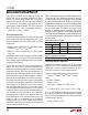
ment. The following information summarized in Table 2
will help optimize power usage.
Table 2. Fault Conditions
INPUT PIN SHDN PIN OUTPUT/SENSE PINS RESULTING CONDITIONS
< V
OUT
(Nominal) Open (High) Forced to V
OUT
(Nominal) Reverse Output Current ≈ 150µA (See Figure 3)
Input Current ≈ 1µA (See Figure 4)
< V
OUT
(Nominal) Grounded Forced to V
OUT
(Nominal) Reverse Output Current ≈ 150µA (See Figure 3)
Input Current ≈ 1µA (See Figure 4)
Open Open (High) > 1V Reverse Output Current ≈ 150µA (See Figure 3)
Open Grounded > 1V Reverse Output Current ≈ 150µA (See Figure 3)
≤ 0.8V Open (High) ≤ 0V Output Current = 0
≤ 0.8V Grounded ≤ 0V Output Current = 0
> 1.5V Open (High) ≤ 0V Output Current = Short-Circuit Current
–15V < V
IN
< 15V Grounded ≤ 0V Output Current = 0
APPLICATIO S I FOR ATIO
WUUU