
Datasheet


6
LT1620/LT1621
APPLICATIONS INFORMATION
WUU
U
TGC
OSC
LTC1435
IN
–
GND
I
OUT
SENSE
IN
+
LT1620MS8
5
6
7
8
4
3
V
BATT
16.8V
V
IN
17.3V TO 28V
LT1620/21 • F02
C11, 56pF
C12, 0.1µF
RUN/SS
I
TH
SFB
SGND
V
OSENSE
SENSE
–
SENSE
+
BOOST
SW
V
IN
INTV
CC
BG
PGND
EXTV
CC
V
CC
PROG
AVG
2
1
C10
100pF
C9, 100pF
R1
1k
C14
1nF
C13
0.033µF
X7R
C17, 0.01µF
R2
1.5M
C4
0.1µF
D2*
D1*
C5, 0.1µF
Si4412DY
Si4412DY
L1
27µH
C6
0.1µF
C7
4.7µF
R
SENSE
0.025Ω
C15
0.1µF
C16
0.1µF
R
P1
3k
1%
R
P2
15.75k
1%
C18
0.1µF
R
F2
110k
0.1%
R
F1
1.44M
0.1%
C8, 100pF
C3
22µF
35V
C1
22µF
35V
C2
22µF
35V
RUN
+ +
+
+
*D1, D2: CENTRAL
SEMICONDUCTOR CMDSH-3
Li-ION
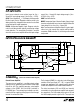
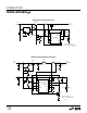
Figure 2. LT1620/LTC1435 Battery Charger
Charge Current Programming
Output current delivered during current mode operation is
determined through programming the voltage at the PROG
pin (V
PROG
). As mentioned above, optimum performance
is obtained with (V
CC
– V
PROG
) = 0.8V. The LT1620 is
biased with a precision 5V supply produced by the LTC1435,
enabling use of a simple resistor divider from V
CC
to
ground for a V
PROG
reference. Using the desired 2.5kΩ
Thevenin impedance at the PROG pin, values of R
P1
= 3k
and R
P2
= 15.75k are readily calculated. The PROG pin
should be decoupled to the V
CC
supply.
Different values of charging current can be obtained by
changing the values of the resistors in the V
PROG
setting
divider to raise or lower the value of the programming
voltage, or by changing the sense resistor to an appropri-
ate value as described above.
Output Float Voltage
The 3.2A charger circuit is designed for a 4-cell Li-Ion
battery, or a battery float voltage of 16.8V. This voltage is
programmed through a resistor divider feedback to the
LTC1435 V
OSENSE
pin, referencing its 1.19V bandgap
voltage. Resistor values are determined through the rela-
tion: R
F1
= (V
BATT
– 1.19)/(1.19/R
F2
). Setting R
F2
= 110k
yields R
F1
= 1.44M.
Other Decoupling Concerns
The application schematic shown in Figure 2 employs
several additional decoupling capacitors. Due to the inher-
ently noisy environment created in switching applications,
decoupling of sensitive nodes is prudent. As noted in the
schematic, decoupling capacitors are included on the
current programming pin (PROG) to the V
CC
rail and