
Datasheet


8
LT1620/LT1621
APPLICATIONS INFORMATION
WUU
U
reduces battery charging current until the external load
subsides.
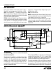
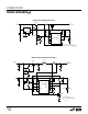
In Figure 4 the LT1620 is coupled with an LT1513 SEPIC
battery charger IC to create an input overcurrent protected
charger circuit.
The programming voltage (V
CC
– V
PROG
) is set to 1.0V
through a resistor divider (R
P1
and R
P2
) from the 5V input
supply to ground. In this configuration, if the input current
drawn by the battery charger
combined
with the system
load requirements exceeds a current limit threshold of 3A,
the battery charger current will be reduced by the LT1620
such that the total
input
supply current is limited to 3A.
Refer to the LT1513 data sheet for additional information.
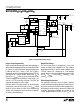
PROGRAMMING ACCURACY CONSIDERATIONS
PWM Controller Error Amp Maximum Source Current
In a typical battery charger application, the LT1620 con-
trols charge current by servoing the error amplifier output
pin of the associated PWM controller IC. Current mode
control is achieved when the LT1620 sinks all of the
current available from the error amplifier. Since the LT1620
has finite transconductance, the voltage required to gen-
erate its necessary output current translates to input
offset error. The LT1620 is designed for a typical I
OUT
sink
current of 130µA to help reduce this term. Knowing the
current source capability of the associated PWM control-
ler in a given application will enable adjustment of the
required programming voltage to accommodate the de-
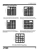
sired charge current. A plot of typical V
PROG
voltage offset
vs PWM source capability is shown in Figure 5a. For
example, the LTC1435 has a current source capability of
about 75µA. This translates to about –15mV of induced
programming offset at V
PROG
(the absolute voltage at the
PROG pin must be 15mV lower).
V
CC
– V
PROG
Programmed Voltage ≠ 0.8V
The LT1620 sense amplifier circuit has an inherent input
referred 3mV offset when IN
+
– IN
–
= 0V to insure closed-
loop operation during light load conditions. This offset vs
input voltage has a linear characteristic, crossing 0V as
IN
+
– IN
–
= 80mV. The offset is translated to the AVG
output (times a factor of 10), and thus to the programming
voltage V
PROG
. A plot of typical V
PROG
offset voltage vs
IN
+
– IN
–
is pictured in Figure 5b. For example, if the
desired load current corresponds to 100mV across the
sense resistor, the typical offset, at V
PROG
is 7.5mV (the
absolute voltage at the PROG pin must be 7.5mV higher).
This error term should be taken into consideration when
using V
ID
values significantly away from 80mV.
V
CC
– V
PROG2
Programmed Voltage ≠ 1.6V
(LT1620GN Only)
The offset term described above for V
PROG
also affects the
V
PROG2
programming voltage proportionally (times an addi-
tional factor of 2). However, V
PROG2
voltage is typically set
well below the zero offset point of 1.6V, so adjustment for this
term is usually required. A plot of typical V
PROG2
offset
voltage vs IN
+
– IN
–
is pictured in Figure 5c. For example,
setting the V
PROG2
voltage to correspond to IN
+
– IN
–
= 15mV
typically requires an additional –50mV offset (the absolute
voltage at the PROG2 pin must be 50mV lower).
Sense Amplifier Input Common Mode < (V
CC
– 0.5V)
The LT1620 sense amplifier has additional input offset
tolerance when the inputs are pulled significantly below
the V
CC
supply. The amplifier can induce additional input
referred offset of up to 11mV when the inputs are at 0V
common-mode. This additional offset term reduces roughly
linearly to zero when V
CM
is about V
CC
– 0.5V. In typical
applications, this offset increases the charge current tol-
erance for “cold start” conditions until V
BAT
moves away
from ground. The resulting output current shift is generally
negative; however, this offset is not precisely controlled.
Precision operation should not be attempted with sense
amplifier common mode inputs below V
CC
– 0.5V. Input
referred offset tolerance vs V
CM
is shown in Figure 5d.
V
CC
≠ 5V
The LT1620 sense amplifier induces a small additional
offset when V
CC
moves away from 5V. This offset follows
a linear characteristic and amounts to about ±0.33mV
(input-referred) over the recommended operating range
of V
CC
, centered at 5V. This offset is translated to the AVG
and AVG2 outputs (times factors of 10 and 20), and thus
to the programming voltages. A plot of programming
offsets vs V
CC
is shown in Figure 5e.