
Datasheet


LT1634
10
1634fe
APPLICATIONS INFORMATION
TYPICAL APPLICATIONS
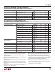
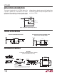
The reverse characteristics of the LT1634 behave like
a resistor in parallel with a Zener diode. This simple,
well behaved characteristic is important to the proper
operation of circuits like Figure 1. The adjustable output
voltage reference depends upon positive feedback from
the LT1495’s output to start-up and regulate the bias cur-
rent for the LT1634.
–
+
LT1495
LT1634-1.25
V
IN
≥ 10.5V
R1
50k TO 1.75M
R2
250k
1634 F01
V
OUT
1.5V TO 10V
R
B
=
V
OUT
– 1.25V
10μA
Figure 1. Adjustable Output Voltage Reference
Reference for Micropower A/D Converter
V
REF
+IN
–IN
GND
8
7
6
5
1
2
3
4
V
CC
CLK
D
OUT
CS/SHDN
LTC1286
V
IN
5V
0.1μF
5V
1634 TA03
18k
LT1634-4.096
μC/μP
SERIAL
INTERFACE
0.1μF
The LT1634-5 Generates the LTC1448 Dual 12-Bit
DAC’s Reference and Supply Voltage
CLK
D
IN
CS/LD
REF
8
7
6
5
1
2
3
4
V
OUTB
V
CC
GND
V
OUTA
LTC1448
7.5V TO 12V
0.1μF
V
OUTB
V
OUTA
1634 TA04
3.48k
LT1634-5
μC/μP
SERIAL
INTERFACE
0.1μF
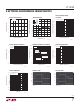
S8 Package
8-Lead Plastic Small Outline (Narrow 0.150 Inch)
(Reference LTC DWG # 05-08-1610)
.016 – .050
(0.406 – 1.270)
.010 – .020
(0.254 – 0.508)
s 45°
0°– 8° TYP
.008 – .010
(0.203 – 0.254)
SO8 0303
.053 – .069
(1.346 – 1.752)
.014 – .019
(0.355 – 0.483)
TYP
.004 – .010
(0.101 – 0.254)
.050
(1.270)
BSC
1
2
3
4
.150 – .15
7
(3.810 – 3.9
8
NOTE 3
8
7
6
5
.189 – .197
(4.801 – 5.004)
NOTE 3
.228 – .244
(5.791 – 6.197)
.160 ±.005
OMMENDED SOLDER PAD LAYOUT
.
045
±
.
005
.050 BSC
.030 ±.005
TYP
INCHES
(MILLIMETERS)
NOTE:
1. DIMENSIONS IN
2. DRAWING NOT TO SCALE
3. THESE DIMENSIONS DO NOT INCLUDE MOLD FLASH OR PROTRUSIONS.
MOLD FLASH OR PROTRUSIONS SHALL NOT EXCEED .006"
(
0.15mm
)
PACKAGE DESCRIPTION