
Datasheet


7
LT1636
1636fc
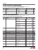
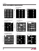
TYPICAL PERFOR A CE CHARACTERISTICS
UW
TOTAL SUPPLY VOLTAGE (V)
0
SUPPLY CURRENT (µA)
40
50
60
40352515545
1636 G01
30
20
0
10 20 30
10
80
70
T
A
= 125°C
T
A
= 25°C
T
A
= –55°C
Supply Current vs Supply Voltage
COMMON MODE VOLTAGE (V)
4.0
–10
INPUT BIAS CURRENT (nA)
0
20
30
40
5.2 10 20 30 40
5000
1636 G03
10
4.4 4.8 50
1000
3000
V
S
= 5V, 0V
T
A
= –55°C
T
A
= 125°C
T
A
= 25°C
Input Bias Current
vs Common Mode Voltage
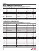
SOURCING LOAD CURRENT (mA)
0.0001 0.001
0.01
OUTPUT SATURATION VOLTAGE (V)
0.1
1
0.01 0.1 1 10 100
1636 G04
V
S
= 5V
V
OD
= 30mV
T
A
= 125°C
T
A
= 25°C
T
A
= –55°C
Output Saturation Voltage
vs Load Current (Output High)
INPUT OVERDRIVE (mV)
0
OUTPUT SATURATION VOLTAGE (mV)
60
80
100
80
1636 G06
40
20
50
70
90
30
10
0
20
40
60
10 90
30
50
70
100
OUTPUT HIGH
OUTPUT LOW
V
S
= ± 2.5V
NO LOAD
Output Saturation Voltage
vs Input Overdrive
Output Saturation Voltage
vs Load Current (Output Low)
SINKING LOAD CURRENT (mA)
0.0001 0.001
0.001
0.01
OUTPUT SATURATION VOLTAGE (V)
0.1
1
10
0.01 0.1 1 10 100
1636 G05
V
S
= 5V
V
OD
= 30mV
T
A
= 125°C
T
A
= –55°C
T
A
= 25°C
Minimum Supply Voltage
TOTAL SUPPLY VOLTAGE (V)
CHANGE IN INPUT OFFSET VOLTAGE (µV)
–300
–100
300
–200
200
100
0
1234
1636 G02
50
T
A
= –55°CT
A
= 125°C
T
A
= 25°C
Note 1: Absolute Maximum Ratings are those values beyond which the life
of a device may be impaired.
Note 2: A heat sink may be required to keep the junction temperature
below absolute maximum. The θ
JA
specified for the DD package is with
minimal PCB heat spreading metal. A significant reduction in θ
JA
can be
obtained with expanded PCB metal area on all layers of a board.
Note 3: The LT1636C and LT1636I are guaranteed functional over the
operating temperature range of –40°C to 85°C. The LT1636H is
guaranteed functional over the operating temperature range of –40°C to
125°C.
Note 4: The LT1636C is guaranteed to meet specified performance from
0°C to 70°C. The LT1636C is designed, characterized and expected to
meet specified performance from –40°C to 85°C but is not tested or QA
sampled at these temperatures. The LT1636I is guaranteed to meet
specified performance from –40°C to 85°C. The LT1636H is guaranteed to
meet specified performance from –40°C to 125°C.
Note 5: V
S
= 5V limits are guaranteed by correlation to V
S
= 3V and
V
S
= ±15V or V
S
= ±22V tests.
Note 6: V
S
= 3V limits are guaranteed by correlation to V
S
= 5V and
V
S
= ±15V or V
S
= ±22V tests.
Note 7: Guaranteed by correlation to slew rate at V
S
= ±15V and GBW at
V
S
= 3V and V
S
= ±15V tests.
Note 8: This specification implies a typical input offset voltage of 600µV at
V
CM
= 44V and a maximum input offset voltage of 3mV at V
CM
= 44V.
Note 9: This parameter is not 100% tested.
ELECTRICAL CHARACTERISTICS