
Datasheet


7
LT1640L/LT1640H
1640lhfb
APPLICATIONS INFORMATION
WUU
U
Hot Circuit Insertion
When circuit boards are inserted into a live – 48V backplane,
the bypass capacitors at the input of the board’s power
module or switching power supply can draw huge tran-
sient currents as they charge up. The transient currents
can cause permanent damage to the board’s components
and cause glitches on the system power supply.
The LT1640 is designed to turn on a board’s supply
voltage in a controlled manner, allowing the board to be
safely inserted or removed from a live backplane. The chip
also provides undervoltage, overvoltage and overcurrent
protection while keeping the power module off until its
input voltage is stable and within tolerance.
+
V
EE
V
DD
LT1640H PWRGD
UV = 37V
OV = 71V
SENSE
C1
150nF
25V
C3
0.1µF
100V
C4
100µF
100V
C5
100µF
16V
Q1
IRF530
R2
10Ω
5%
R3
18k
5%
C2
3.3nF
100V
R4
562k
1%
R5
9.09k
1%
R6
10k
1%
R1
0.02Ω
5%
4
3
2
OV
GND
GND
–48V
UV
56
8
7
1
GATE DRAIN
VICOR
VI-J3D-CY
V
OUT
+
V
OUT
–
V
IN
+
5V
1640 F06a
GATE IN
V
IN
–
+
(SHORT PIN)
*
* DIODES INC. SMAT70A
2× 1N4148
43
21
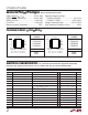
Power Supply Ramping
The input to the power module on a board is controlled by
placing an external N-channel pass transistor (Q1) in the
power path (Figure 6a, all waveforms are with respect to
the V
EE
pin of the LT1640). R1 provides current fault
detection and R2 prevents high frequency oscillations.
Resistors R4, R5 and R6 provide undervoltage and over-
voltage sensing. By ramping the gate of Q1 up at a slow
rate, the surge current charging load capacitors C3 and C4
can be limited to a safe value when the board makes
connection.
Resistor R3 and capacitor C2 act as a feedback network to
accurately control the inrush current. The inrush current
can be calculated with the following equation:
I
INRUSH
= (45µA • C
L
)/C2
where C
L
is the total load capacitance, C3 + C4 + module
input capacitance.
Figure 6a. Inrush Control Circuitry