
Datasheet


LT1715
4
1715fa
ELECTRICAL CHARACTERISTICS
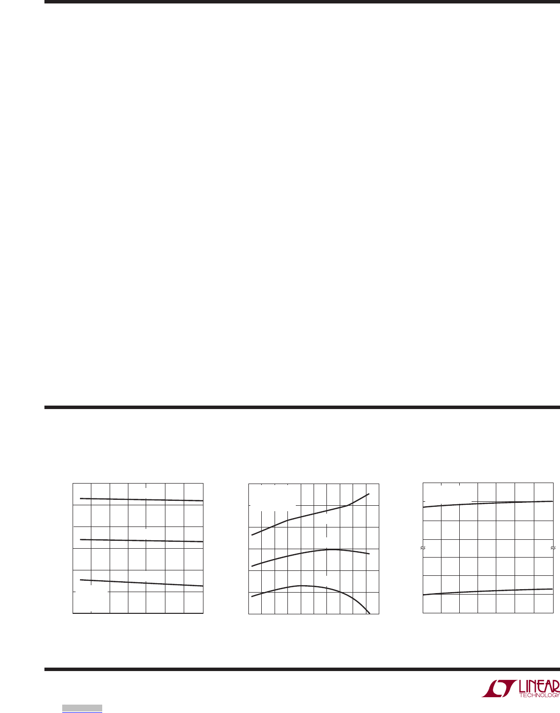
Input Offset and Trip Voltages
vs Supply Voltage
Input Offset and Trip Voltages
vs Temperature
Input Common Mode Limits
vs Temperature
SUPPLY VOLTAGE, V
CC
= +V
S
(V)
2.5
V
OS
AND TRIP POINT VOLTAGE (mV)
3
2
1
0
–1
–2
–3
4.0 5.0
1715 G01
3.0 3.5
4.5 5.5 6.0
V
TRIP
+
V
OS
V
TRIP
–
T
A
= 25°C
V
CM
= 1V
V
EE
= GND
TEMPERATURE (°C)
–3
V
OS
AND TRIP POINT VOLTAGE (mV)
–1
1
3
–2
0
2
–20 20 60 100
1715 G02
140–40–60 0 40 80 120
V
TRIP
+
V
OS
V
TRIP
–
+V
S
= V
CC
= 5V
V
CM
= 1V
V
EE
= –5V
TEMPERATURE (°C)
–50
3.6
3.8
4.2
25 75
1715 G03
–4.8
–5.0
–25 0
50 100 125
–5.2
–5.4
4.0
COMMON MODE INPUT VOLTAGE (V)
+V
S
= V
CC
= 5V
V
EE
= –5V
Note 1: Stresses beyond those listed under Absolute Maximum Ratings
may cause permanent damage to the device. Exposure to any Absolute
Maximum Rating condition for extended periods may affect device
reliability and lifetime.
Note 2: The LT1715C is guaranteed functional over the operating range of
–40°C to 85°C.
Note 3: The LT1715C is guaranteed to meet specifi ed performance from
0°C to 70°C. The LT1715°C is designed, characterized and expected to
meet specifi ed performance from –40°C to 85°C but is not tested or
QA sampled at these temperatures. The LT1715I is guaranteed to meet
specifi ed performance from –40°C to 85°C. The LT1715H is guaranteed to
meet specifi ed performance from –40°C to 125°C.
Note 4: Thermal resistances vary depending upon the amount of PC board
metal attached to Pin 5 of the device. θ
JA
is specifi ed for a 2500mm
2
3/32"
FR-4 board covered with 2oz copper on both sides and with 100mm
2
of
copper attached to Pin 5. Thermal performance can be improved beyond
the given specifi cation by using a 4-layer board or by attaching more metal
area to Pin 5.
Note 5: If one input is within these common mode limits, the other input
can go outside the common mode limits and the output will be valid.
Note 6: The LT1715 comparator includes internal hysteresis. The trip
points are the input voltage needed to change the output state in each
direction. The offset voltage is defi ned as the average of V
TRIP
+
and V
TRIP
–
,
while the hysteresis voltage is the difference of these two.
Note 7: The common mode rejection ratio is measured with V
CC
= 5V,
V
EE
= –5V and is defi ned as the change in offset voltage measured from
V
CM
= –5.1V to V
CM
= 3.8V, divided by 8.9V.
Note 8: The power supply rejection ratio is measured with V
CM
= 1V and is
defi ned as the worst of: the change in offset voltage from V
CC
= +V
S
= 2.7V
to V
CC
= +V
S
= 6V (with V
EE
= 0V) divided by 3.3V or the change in offset
voltage from V
EE
= 0V to V
EE
= –6V (with V
CC
= +V
S
= 6V) divided by 6V.
Note 9: Because of internal hysteresis, there is no small-signal region in
which to measure gain. Proper operation of internal circuity is ensured by
measuring V
OH
and V
OL
with only 20mV of overdrive.
Note 10: Maximum toggle rate is defi ned as the highest frequency at
which a 100mV sinusoidal input results in an error free output toggling to
greater than 4V when high and to less than 1V when low on a 5V output
supply.
Note 11: Propagation delay measurements made with 100mV steps.
Overdrive is measured relative to V
TRIP
±
.
Note 12: t
PD
cannot be measured in automatic handling equipment with
low values of overdrive. The LT1715 is 100% tested with a 100mV step
and 20mV overdrive. Correlation tests have shown that t
PD
limits can be
guaranteed with this test.
Note 13: Propagation Delay Skew is defi ned as:
t
SKEW
= |t
PDLH
– t
PDHL
|
Note 14: Differential propagation delay is defi ned as the larger of the two:
Δt
PDLH
= |t
PDLHA
– t
PDLHB
|
Δt
PDHL
= |t
PDHLA
– t
PDHLB
|
Note 15: Package inductances combined with asynchronous activity on
the other channel can increase the output jitter. See Channel Interactions
in Applications Information. Specifi cation above is with one channel active
only.
TYPICAL PERFORMANCE CHARACTERISTICS
Downloaded from Arrow.com.Downloaded from Arrow.com.Downloaded from Arrow.com.Downloaded from Arrow.com.