
Datasheet


LT1720/LT1721
1
17201fc
TYPICAL APPLICATION
DESCRIPTION
Dual/Quad, 4.5ns, Single
Supply 3V/5V Comparators
with Rail-to-Rail Outputs
The LT
®
1720/LT1721 are UltraFast
TM
dual/quad compara-
tors optimized for single supply operation, with a supply
voltage range of 2.7V to 6V. The input voltage range extends
from 100mV below ground to 1.2V below the supply volt-
age. Internal hysteresis makes the LT1720/LT1721 easy to
use even with slow moving input signals. The rail-to-rail
outputs directly interface to TTL and CMOS. Alternatively,
the symmetric output drive can be harnessed for analog
applications or for easy translation to other single supply
logic levels.
The LT1720 is available in three 8-pin packages; three pins
per comparator plus power and ground. In addition to SO
and MSOP packages, a 3mm × 3mm low profi le (0.8mm)
dual fi ne pitch leadless package (DFN) is available for space
limited applications. The LT1721 is available in the 16-pin
SSOP and S packages.
The pinouts of the LT1720/LT1721 minimize parasitic
effects by placing the most sensitive inputs (inverting)
away from the outputs, shielded by the power rails. The
LT1720/LT1721 are ideal for systems where small size and
low power are paramount.
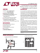
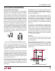
2.7V to 6V Crystal Oscillator with TTL/CMOS Output
L, LT, LTC and LTM are registered trademarks of Linear Technology Corporation. UltaFast is
a trademark of Linear Technology Corporation. All other trademarks are the property of their
respective owners.
FEATURES
APPLICATIONS
n
High Speed Differential Line Receiver
n
Crystal Oscillator Circuits
n
Window Comparators
n
Threshold Detectors/Discriminators
n
Pulse Stretchers
n
Zero-Crossing Detectors
n
High Speed Sampling Circuits
n
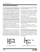
UltraFast: 4.5ns at 20mV Overdrive
7ns at 5mV Overdrive
n
Low Power: 4mA per Comparator
n
Optimized for 3V and 5V Operation
n
Pinout Optimized for High Speed Ease of Use
n
Input Voltage Range Extends 100mV
Below Negative Rail
n
TTL/CMOS Compatible Rail-to-Rail Outputs
n
Internal Hysteresis with Specifi ed Limits
n
Low Dynamic Current Drain; 15μA/(V-MHz),
Dominated by Load In Most Circuits
n
Tiny 3mm × 3mm × 0.75mm DFN Package (LT1720)
Propagation Delay vs Overdrive
–
+
C1
1/2 LT1720
2.7V TO 6V
2k
620Ω
220Ω
1MHz TO 10MHz
CRYSTAL (AT-CUT)
2k
17201 TA01
0.1μF 1.8k
OUTPUT
GROUND
CASE
OVERDRIVE (mV)
0
DELAY (ns)
30
50
17201 TA02
10 20 40
8
7
6
5
4
3
2
1
0
25°C
V
STEP
= 100mV
V
CC
= 5V
C
LOAD
= 10pF
RISING EDGE
(t
PDLH
)
FALLING EDGE
(t
PDHL
)