
Datasheet


LT1763 Series
15
1763fg
The LT1763 series are 500mA low dropout regulators with
micropower quiescent current and shutdown. The devices
are capable of supplying 500mA at a dropout voltage of
300mV. Output voltage noise can be lowered to 20μV
RMS
over a 10Hz to 100kHz bandwidth with the addition of
a 0.01μF reference bypass capacitor. Additionally, the
reference bypass capacitor will improve transient response
of the regulator, lowering the settling time for transient load
conditions. The low operating quiescent current (30μA)
drops to less than 1μA in shutdown. In addition to the
low quiescent current, the LT1763 regulators incorporate
several protection features which make them ideal for use
in battery-powered systems. The devices are protected
against both reverse input and reverse output voltages.
In battery backup applications where the output can be
held up by a backup battery when the input is pulled to
ground, the LT1763-X acts like it has a diode in series with
its output and prevents reverse current fl ow. Additionally,
in dual supply applications where the regulator load is
returned to a negative supply, the output can be pulled
below ground by as much as 20V and still allow the device
to start and operate.
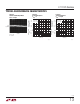
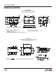
Adjustable Operation
The adjustable version of the LT1763 has an output voltage
range of 1.22V to 20V. The output voltage is set by the
ratio of two external resistors, as shown in Figure 2. The
device servos the output to maintain the ADJ pin voltage
at 1.22V referenced to ground. The current in R1 is then
equal to 1.22V/R1 and the current in R2 is the current
in R1 plus the ADJ pin bias current. The ADJ pin bias
current, 30nA at 25°C, fl ows through R2 into the ADJ pin.
The output voltage can be calculated using the formula in
Figure 2. The value of R1 should be no greater than 250k
to minimize errors in the output voltage caused by the
ADJ pin bias current. Note that in shutdown the output
is turned off and the divider current will be zero. Curves
of ADJ Pin Voltage vs Temperature and ADJ Pin Bias
Current vs Temperature appear in the Typical Performance
Characteristics section.
The adjustable device is tested and specifi ed with the ADJ
pin tied to the OUT pin for an output voltage of 1.22V.
Specifi cations for output voltages greater than 1.22V will
be proportional to the ratio of the desired output voltage
APPLICATIONS INFORMATION
Figure 2. Adjustable Operation
to 1.22V: V
OUT
/1.22V. For example, load regulation for an
output current change of 1mA to 500mA is –2mV typical
at V
OUT
= 1.22V. At V
OUT
= 12V, load regulation is:
(12V/1.22V)(–2mV) = –19.6mV
Bypass Capacitance and Low Noise Performance
The LT1763 regulators may be used with the addition of
a bypass capacitor from V
OUT
to the BYP pin to lower
output voltage noise. A good quality low leakage capacitor
is recommended. This capacitor will bypass the reference
of the regulator, providing a low frequency noise pole.
The noise pole provided by this bypass capacitor will
lower the output voltage noise to as low as 20μV
RMS
with the addition of a 0.01μF bypass capacitor. Using
a bypass capacitor has the added benefi t of improving
transient response. With no bypass capacitor and a 10μF
output capacitor, a 10mA to 500mA load step will settle
to within 1% of its fi nal value in less than 100μs. With
the addition of a 0.01μF bypass capacitor, the output will
settle to within 1% for a 10mA to 500mA load step in less
than 10μs, with total output voltage deviation of less than
2.5% (see the LT1763-5 Transient Response curve in the
Typical Performance Characteristics section). However,
regulator start-up time is proportional to the size of the
bypass capacitor, slowing to 15ms with a 0.01μF bypass
capacitor and 10μF output capacitor.
IN
1763 F02
R2
OUT
V
IN
V
OUT
ADJ
GND
LT1763
R1
+
VV
R
R
IR
VV
InA
OUT ADJ
ADJ
ADJ
=+
⎛
⎝
⎜
⎞
⎠
⎟
+
()()
=
=°
122 1
2
1
2
122
30
.
.
AT 25 C
OUTPUT RANGE = 1.22V TO 20V