
Datasheet


LT1763 Series
19
1763fg
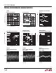
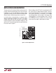
Figure 7. Reverse Output Current
The top resistor of the resistor divider must be chosen to
limit the current into the ADJ pin to less than 5mA when
the ADJ pin is at 7V. The 13V difference between output
and ADJ pin divided by the 5mA maximum current into the
ADJ pin yields a minimum top resistor value of 2.6k.
In circuits where a backup battery is required, several
different input/output conditions can occur. The output
voltage may be held up while the input is either pulled
to ground, pulled to some intermediate voltage or is left
open-circuit. Current fl ow back into the output will follow
the curve shown in Figure 7.
When the IN pin of the LT1763-X is forced below the OUT
pin, or the OUT pin is pulled above the IN pin, input cur-
rent will typically drop to less than 2μA. This can happen
if the input of the device is connected to a discharged
(low voltage) battery and the output is held up by either
a backup battery or a second regulator circuit. The state
of the SHDN pin will have no effect on the reverse output
current when the output is pulled above the input.
OUTPUT VOLTAGE (V)
100
90
80
70
60
50
40
30
20
10
0
REVERSE OUTPUT CURRENT (μA)
1763 F07
0123
4
5
678910
T
J
= 25°C
V
IN
= 0V
CURRENT FLOWS
INTO OUTPUT PIN
V
OUT
= V
ADJ
(LT1763)
LT1763
LT1763-5
LT1763-3.3
LT1763-1.5
LT1763-1.8
LT1763-2.5
LT1763-3
APPLICATIONS INFORMATION