
Datasheet


12
LT1764 Series
1764fb
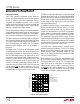
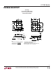
Figure 4. Ceramic Capacitor Temperature Characteristics
The protection is designed to provide some output current
at all values of input-to-output voltage up to the device
breakdown.
When power is first turned on, as the input voltage rises,
the output follows the input, allowing the regulator to start
up into very heavy loads. During the start-up, as the input
voltage is rising, the input-to-output voltage differential is
small, allowing the regulator to supply large output cur-
rents. With a high input voltage, a problem can occur
wherein removal of an output short will not allow the
output voltage to recover. Other regulators, such as the
LT1085, also exhibit this phenomenon, so it is not unique
to the LT1764 series.
The problem occurs with a heavy output load when the
input voltage is high and the output voltage is low. Com-
mon situations are immediately after the removal of a
short circuit or when the SHDN pin is pulled high after the
input voltage has already been turned on. The load line for
such a load may intersect the output current curve at two
points. If this happens, there are two stable output oper-
ating points for the regulator. With this double intersec-
tion, the input power supply may need to be cycled down
to zero and brought up again to make the output recover.
Output Voltage Noise
The LT1764 regulators have been designed to provide low
output voltage noise over the 10Hz to 100kHz bandwidth
while operating at full load. Output voltage noise is typi-
cally 50nV√Hz over this frequency bandwidth for the
LT1764 (adjustable version). For higher output voltages
(generated by using a resistor divider), the output voltage
noise will be gained up accordingly. This results in RMS
noise over the 10Hz to 100kHz bandwidth of 15µV
RMS
for
the LT1764 increasing to 37µV
RMS
for the LT1764-3.3.
Higher values of output voltage noise may be measured
when care is not exercised with regards to circuit layout
and testing. Crosstalk from nearby traces can induce
unwanted noise onto the output of the LT1764-X. Power
supply ripple rejection must also be considered; the LT1764
regulators do not have unlimited power supply rejection
and will pass a small portion of the input noise through to
the output.
TEMPERATURE (°C)
–50
40
20
0
–20
–40
–60
–80
–100
25 75
1764 F04
–25 0
50 100 125
Y5V
CHANGE IN VALUE (%)
X5R
BOTH CAPACITORS ARE 16V,
1210 CASE SIZE, 10µF
APPLICATIO S I FOR ATIO
WUUU
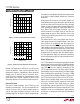
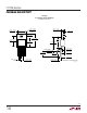
Figure 3. Ceramic Capacitor DC Bias Characteristics
DC BIAS VOLTAGE (V)
CHANGE IN VALUE (%)
1764 F03
20
0
–20
–40
–60
–80
–100
0
4
8
10
26
12
14
X5R
Y5V
16
BOTH CAPACITORS ARE 16V,
1210 CASE SIZE, 10µF
Voltage and temperature coefficients are not the only
sources of problems. Some ceramic capacitors have a
piezoelectric response. A piezoelectric device generates
voltage across its terminals due to mechanical stress,
similar to the way a piezoelectric accelerometer or micro-
phone works. For a ceramic capacitor the stress can be
induced by vibrations in the system or thermal transients.
Overload Recovery
Like many IC power regulators, the LT1764-X has safe
operating area protection. The safe area protection de-
creases the current limit as input-to-output voltage in-
creases and keeps the power transistor inside a safe
operating region for all values of input-to-output voltage.