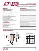
LT1766/LT1766-5 5.5V to 60V 1.5A, 200kHz Step-Down Switching Regulator FEATURES DESCRIPTION n The LT®1766/LT1766-5 are 200kHz monolithic buck switching regulators that accept input voltages up to 60V. A high efficiency 1.5A, 0.2Ω switch is included on the die along with all the necessary oscillator, control and logic circuitry. A current mode control architecture delivers fast transient response and excellent loop stability. n n n n n n n n n n n Wide Input Range: 5.5V to 60V 1.
LT1766/LT1766-5 ABSOLUTE MAXIMUM RATINGS (Note 1) Input Voltage (VIN) .................................................. 60V BOOST Pin Above SW .............................................. 35V BOOST Pin Voltage ................................................. 68V SYNC, SENSE Voltage (LT1766-5) ............................. 7V SHDN Voltage ............................................................ 6V BIAS Pin Voltage .....................................................
LT1766/LT1766-5 ORDER INFORMATION LEAD FREE FINISH TAPE AND REEL PART MARKING PACKAGE DESCRIPTION TEMPERATURE RANGE LT1766EFE#PBF LT1766EFE#TRPBF 1766EFE 16-Lead Plastic TSSOP 0°C to 125°C LT1766IFE#PBF LT1766IFE#TRPBF 1766IFE 16-Lead Plastic TSSOP –40°C to 125°C LT1766HFE#PBF LT1766HFE#TRPBF 1766HFE 16-Lead Plastic TSSOP –40°C to 140°C LT1766EFE-5#PBF LT1766EFE-5#TRPBF 1766EFE-5 16-Lead Plastic TSSOP 0°C to 125°C LT1766IFE-5#PBF LT1766IFE-5#TRPBF 1766IFE-5 16-Lead Plastic TSSOP
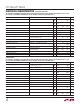
LT1766/LT1766-5 ELECTRICAL CHARACTERISTICS (LT1766E/LT1766I Grade) The l denotes specifications which apply over the full operating temperature range, otherwise specifications are at TJ = 25°C. VIN = 15V, VC = 1.5V, SHDN = 1V, BOOST open circuit, SW open circuit, unless otherwise noted. PARAMETER CONDITIONS Switch On-Resistance ISW = 1.5A, Boost = VIN + 5V (Note 7) Maximum Switch Duty Cycle FB = 1V or VSENSE = 4.1V Switch Frequency VC Set to Give DC = 50% fSW Line Regulation 5.
LT1766/LT1766-5 ELECTRICAL CHARACTERISTICS (LT1766H Grade) The l denotes specifications which apply over the full operating temperature range, otherwise specifications are at TJ = 25°C. VIN = 15V, VC = 1.5V, SHDN = 1V, BOOST open circuit, SW open circuit, unless otherwise noted. PARAMETER CONDITIONS fSW Line Regulation 5.5V ≤ VIN ≤ 60V MIN TYP MAX UNITS l 0.05 0.15 %/V fSW Frequency Shifting Threshold Df = 10kHz Minimum Input Voltage (Note 3) l 4.6 5.
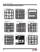
LT1766/LT1766-5 TYPICAL PERFORMANCE CHARACTERISTICS SHDN Pin Bias Current FB Pin Voltage and Current Switch Peak Current Limit 2.5 1.234 TA = 25°C 2.0 250 VOLTAGE 1.219 1.0 CURRENT 1.214 CURRENT (μA) FEEDBACK VOLTAGE (V) GUARANTEED MINIMUM 1.5 1.5 1.224 CURRENT (μA) SWITCH PEAK CURRENT (A) TYPICAL 2.0 150 100 0 20 40 60 DUTY CYCLE (%) 80 0 25 50 75 100 125 150 0 JUNCTION TEMPERATURE (°C) 1766 G01 Shutdown Supply Current 1.6 1.2 0.8 START-UP 0.
LT1766/LT1766-5 TYPICAL PERFORMANCE CHARACTERISTICS Minimum Input Voltage with 5V Output Switching Frequency 7.5 230 BOOST Pin Current 45 TA = 25°C TA = 25°C 40 210 200 190 6.5 MINIMUM INPUT VOLTAGE TO START 6.0 MINIMUM INPUT VOLTAGE TO RUN 5.5 180 0 25 50 75 100 125 5.0 150 0 JUNCTION TEMPERATURE (°C) 0.1 0.2 0.3 0.4 0.5 0.6 0.7 0.8 0.9 LOAD CURRENT (A) 1766 G10 25 20 15 10 0 1 2.1 450 1.9 400 1.7 1.5 1.3 1.1 0.5 1 SWITCH CURRENT (A) 1.
LT1766/LT1766-5 PIN FUNCTIONS VIN (Pin 4): This is the collector of the on-chip power NPN switch. VIN powers the internal control circuitry when a voltage on the BIAS pin is not present. High dI/dt edges occur on this pin during switch turn on and off. Keep the path short from the VIN pin through the input bypass capacitor, through the catch diode back to SW. All trace inductance on this path will create a voltage spike at switch off, adding to the VCE voltage across the internal NPN.
LT1766/LT1766-5 BLOCK DIAGRAM will have 90° phase shift at a much lower frequency, but will not have the additional 90° shift until well beyond the LC resonant frequency. This makes it much easier to frequency compensate the feedback loop and also gives much quicker transient response. output voltage). This will improve efficiency if the BIAS pin voltage is lower than regulator input voltage.
LT1766/LT1766-5 APPLICATIONS INFORMATION FEEDBACK PIN FUNCTIONS The feedback (FB) pin on the LT1766 is used to set output voltage and provide several overload protection features. The first part of this section deals with selecting resistors to set output voltage and the remaining part talks about foldback frequency and current limiting created by the FB pin. Please read both parts before committing to a final design.
LT1766/LT1766-5 APPLICATIONS INFORMATION LT1766 VSW TO FREQUENCY SHIFTING 1.4V – OUTPUT 5V Q1 ERROR AMPLIFIER + L1 R1 1.2V R4 2k R3 1k FB + C1 BUFFER Q2 R2 5k TO SYNC CIRCUIT VC GND 1766 F02 Figure 2. Frequency and Current Limit Foldback divider impedance is not critical, caution should be used if resistors are increased beyond the suggested values and short-circuit conditions occur with high input voltage.
LT1766/LT1766-5 APPLICATIONS INFORMATION where: ESR = equivalent series resistance of the output capacitor ESL = equivalent series inductance of the output capacitor dI/dt = slew rate of inductor ripple current = VIN/L Peak-to-peak ripple current (ILP-P) through the inductor and into the output capacitor is typically chosen to be between 20% and 40% of the maximum load current. It is approximated by: ILP-P = ( VOUT )( VIN – VOUT ) ( VIN )( f)(L) )( VENDOR/ PART NO. ) 40 dI = = 10 6 • 0.
LT1766/LT1766-5 APPLICATIONS INFORMATION the high side for discontinuous mode, so it can be used for all conditions. IPEAK = IOUT + ( )( ) ( )( )( )( ) VOUT VIN – VOUT (ILP-P ) = IOUT + 2 2 VIN f L EMI Decide if the design can tolerate an open core geometry like a rod or barrel, which have high magnetic field radiation, or whether it needs a closed core like a toroid to prevent EMI problems.
LT1766/LT1766-5 APPLICATIONS INFORMATION Discontinuous mode is entered when the output load current is less than one-half of the inductor ripple current (ILP-P). In this mode, inductor current falls to zero before the next switch turn on (see Figure 8).
LT1766/LT1766-5 APPLICATIONS INFORMATION frequency decreases roughly linearly down to a limit of about 40kHz. This lower oscillator frequency during short-circuit conditions can then maintain control with the effective minimum on time. capacitors fail during very high turn-on surges, which do not occur at the output of regulators. High discharge surges, such as when the regulator output is dead shorted, do not harm the capacitors.
LT1766/LT1766-5 APPLICATIONS INFORMATION INPUT CAPACITOR Step-down regulators draw current from the input supply in pulses. The rise and fall times of these pulses are very fast. The input capacitor is required to reduce the voltage ripple this causes at the input of LT1766 and force the switching current into a tight local loop, thereby minimizing EMI. The RMS ripple current can be calculated from: IRIPPLE(RMS) = IOUT VOUT ( VIN – VOUT ) / VIN2 Ceramic capacitors are ideal for input bypassing.
LT1766/LT1766-5 APPLICATIONS INFORMATION BOOST PIN For most applications, the boost components are a 0.33μF capacitor and a 1N4148W diode. The anode is typically connected to the regulated output voltage to generate a voltage approximately VOUT above VIN to drive the output stage. However, the output stage discharges the boost capacitor during the on time of the switch. The output driver requires at least 3V of headroom throughout this period to keep the switch fully saturated.
LT1766/LT1766-5 APPLICATIONS INFORMATION Keep the connections from the resistors to the shutdown pin short and make sure that interplane or surface capacitance to the switching nodes are minimized. If high resistor values are used, the shutdown pin should be bypassed with a 1000pF capacitor to prevent coupling problems from the switch node. If hysteresis is desired in the undervoltage lockout point, a resistor, RFB, can be added to the output node.
LT1766/LT1766-5 APPLICATIONS INFORMATION CONNECT TO GROUND PLANE GND L1 C1 MINIMIZE LT1766 C3-D1 LOOP GND D2 D1 VOUT C2 1 GND 15 3 14 4 VIN C3 5 LT1766 6 BOOST VIN GND 16 2 SW 13 SHDN FOR THE FE PACKAGE, THE EXPOSED PAD (PIN 17) SHOULD BE PROPERLY SOLDERED TO THE GROUND PLANE.
LT1766/LT1766-5 APPLICATIONS INFORMATION SW RISE SW FALL 10V/DIV SWITCH NODE VOLTAGE 0.2A/DIV INDUCTOR CURRENT AT IOUT = 0.1A 2V/DIV 50ns/DIV VIN = 40V VOUT = 5V L = 47μH 1766 F07 Figure 7. Switch Node Resonance a >100MHz oscilloscope must be used, and waveforms should be observed on the leads of the package. This switch off spike will also cause the SW node to go below ground. The LT1766 has special circuitry inside which mitigates this problem, but negative voltages over 0.
LT1766/LT1766-5 APPLICATIONS INFORMATION Thermal resistance for the LT1766 packages is influenced by the presence of internal or backside planes. SSOP (GN16) package: With a full plane under the GN16 package, thermal resistance will be about 85°C/W. TSSOP (exposed pad) package: With a full plane under the TSSOP package, thermal resistance will be about 45°C/W.
LT1766/LT1766-5 APPLICATIONS INFORMATION For output voltages of 5V, VC2 is approximately 5V. During switch turn on, VC2 will fall as the boost capacitor C2 is dicharged by the BOOST pin. In the previous BOOST Pin section, the value of C2 was designed for a 0.7V droop in VC2 = VDROOP . Hence, an output voltage as low as 4V would still allow the minimum 3.3V for the boost function using the C2 capacitor calculated.
LT1766/LT1766-5 APPLICATIONS INFORMATION 1. Be aware that the simultaneous requirements of high VIN, high IOUT and high fOSC may not be achievable in practice due to internal dissipation. The Thermal Considerations section offers a basis to estimate internal power. In questionable cases a prototype supply should be built and exercised to verify acceptable operation.
LT1766/LT1766-5 APPLICATIONS INFORMATION When using RC, the maximum value has two limitations. First, the combination of output capacitor ESR and RC may stop the loop rolling off altogether. Second, if the loop gain is not rolled off sufficiently at the switching frequency, output ripple will peturb the VC pin enough to cause unstable duty cycle switching similar to subharmonic oscillations.
LT1766/LT1766-5 APPLICATIONS INFORMATION (R4)(CSS )(VOUT ) RiseTime = VBE Using the values shown in Figure 10, 47 • 103 )(15 • 10–9 )(5) ( Rise Time = = 5ms 0.7 The ramp is linear and rise times in the order of 100ms are possible. Since the circuit is voltage controlled, the ramp rate is unaffected by load characteristics and maximum output current is unchanged. Variants of this circuit can be used for sequencing multiple regulator outputs. D2 1N4148W INPUT 40V BOOST C3 2.2μF 50V CER C2 0.
LT1766/LT1766-5 APPLICATIONS INFORMATION IP = Maximum rated switch current VIN = Minimum input voltage VOUT = Output voltage VF = Catch diode forward voltage 0.3 = Switch voltage drop at 1.5A mode formula to calculate minimum inductor needed. If load current is higher, use the continuous mode formula. Output current where continuous mode is needed: Example: with VIN(MIN) = 5.5V, VOUT = 12V, L = 18μH, VF = 0.63V, IP = 1.5A: IMAX = 0.280A. OUTPUT DIVIDER C2 0.33μF BOOST L1* 18μH VSW VIN GND C3 2.
LT1766/LT1766-5 APPLICATIONS INFORMATION Note 44, pages 29 and 30. For our purposes here a fudge factor (ff) is used. The value for ff is about 1.2 for higher load currents and L ≥15μH. It increases to about 2.0 for smaller inductors at lower load currents. Input Capacitor IRMS = ( ff)(IOUT ) VOUT VIN ff = 1.2 to 2.
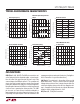
LT1766/LT1766-5 PACKAGE DESCRIPTION FE Package 16-Lead Plastic TSSOP (4.4mm) (Reference LTC DWG # 05-08-1663) Exposed Pad Variation BB 4.90 – 5.10* (.193 – .201) 3.58 (.141) 4.30 – 4.50* (.169 – .177) 6.60 p0.10 0.25 REF 2.94 (.116) 4.50 p0.10 1.10 (.0433) MAX 0.09 – 0.20 (.0035 – .0079) 0.65 (.0256) BSC 0.50 – 0.75 (.020 – .030) 1.05 p0.10 0.65 BSC RECOMMENDED SOLDER PAD LAYOUT NOTE: 1. CONTROLLING DIMENSION: MILLIMETERS MILLIMETERS 2. DIMENSIONS ARE IN (INCHES) 3.
LT1766/LT1766-5 REVISION HISTORY (Revision history begins at Rev C) REV DATE DESCRIPTION C 03/10 Removed LT1766HGN from Order Information PAGE NUMBER 2 1766fc Information furnished by Linear Technology Corporation is believed to be accurate and reliable. However, no responsibility is assumed for its use. Linear Technology Corporation makes no representation that the interconnection of its circuits as described herein will not infringe on existing patent rights.
LT1766/LT1766-5 RELATED PARTS PART NUMBER DESCRIPTION COMMENTS LT1074/LT1074HV 4.4A (IOUT), 100kHz, High Efficiency Step-Down DC/DC Converters VIN: 7.3V to 45V/64V, VOUT(MIN): 2.21V, IQ: 8.5mA, ISD: 10μA, DD-5/7, TO220-5/7 LT1076/LT1076HV 1.6A (IOUT), 100kHz, High Efficiency Step-Down DC/DC Converters VIN: 7.3V to 45V/64V, VOUT(MIN): 2.21V, IQ: 8.5mA, ISD: 10μA, DD-5/7, TO220-5/7 LT1616 500mA (IOUT), 1.4MHz, High Efficiency Step-Down DC/DC Converter VIN: 3.6V to 25V, VOUT(MIN): 1.25V, IQ: 1.