
Datasheet

LT1766/LT1766-5
22
1766fc
APPLICATIONS INFORMATION
For an FE package with thermal resistance of 45°C/W,
ambient temperature savings would be, T(ambient) savings
= 0.116W • 45°C/W = 5c. For a GN Package with thermal
resistance of 85°C/W, ambient temperature savings would
be T/(ambient) savings = 0.116 • 85°C/W = 10c. The 7V
zener should be sized for excess of 0.116W operation. The
tolerances of the zener should be considered to ensure
minimum V
C2
exceeds 3.3V + V
DROOP
.
Input Voltage vs Operating Frequency Considerations
The absolute maximum input supply voltage for the
LT1766 is specifi ed at 60V. This is based solely on internal
semiconductor junction breakdown effects. Due to internal
power dissipation, the actual maximum V
IN
achievable in
a particular application may be less than this.
A detailed theoretical basis for estimating internal power
loss is given in the section, Thermal Considerations. Note
that AC switching loss is proportional to both operating
frequency and output current. The majority of AC switching
loss is also proportional to the
square
of input voltage.
For example, while the combination of V
IN
= 40V, V
OUT
= 5V at 1A and f
OSC
= 200kHz may be easily achievable,
simultaneously raising V
IN
to 60V and f
OSC
to 700kHz is
not possible. Nevertheless, input voltage
transients
up to
60V can usually be accommodated, assuming the result-
ing increase in internal dissipation is of insuffi cient time
duration to raise die temperature signifi cantly.
A second consideration is controllability. A potential limita-
tion occurs with a high step-down ratio of V
IN
to V
OUT
, as
this requires a correspondingly narrow minimum switch
on time. An approximate expression for this (assuming
continuous mode operation) is given as follows:
Min t
VV
Vf
ON
OUT F
IN OSC
=
+
()
where:
V
IN
= Input voltage
V
OUT
= Output voltage
V
F
= Schottky diode forward drop
f
OSC
= Switching frequency
A potential controllability problem arises if the LT1766 is
called upon to produce an on time shorter than it is able
to produce. Feedback loop action will lower then reduce
For output voltages of 5V, V
C2
is approximately 5V. During
switch turn on, V
C2
will fall as the boost capacitor C2 is
dicharged by the BOOST pin. In the previous BOOST Pin
section, the value of C2 was designed for a 0.7V droop in
V
C2
= V
DROOP
. Hence, an output voltage as low as 4V would
still allow the minimum 3.3V for the boost function using
the C2 capacitor calculated. If a target output voltage of
12V is required, however, an excess of 8V is placed across
the boost capacitor which is not required for the boost
function but still dissipates additional power.
What is required is a voltage drop in the path of D2 to
achieve minimal power dissipation while still maintaining
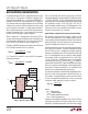
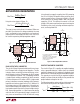
minimum boost voltage across C2. A zener, D4, placed in
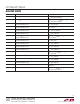
series with D2 (see Figure 9), drops voltage to C2.
Example : the BOOST pin power dissipation for a 20V input
to 12V output conversion at 1A is given by:
PW
BOOST
==
12 1 36 12
20
02
•( / )•
.
If a 7V zener D4 is placed in series with D2, then power
dissipation becomes :
PW
BOOST
==
12 1 36 5
20
0 084
•( / )•
.
BOOST
V
IN
D1
R1
V
OUT
C
F
C
C
LT1766
SHDN
SYNC
SW
BIAS
FB
V
C
GND
C2
C1
L1
D2
R2
1766 F09
C3
V
IN
D2 D4
+
R
C
Figure 9. Boost Pin, Diode Selection