
Datasheet

LT1766/LT1766-5
14
1766fc
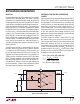
Discontinuous mode is entered when the output load
current is less than one-half of the inductor ripple current
(I
LP-P
). In this mode, inductor current falls to zero before
the next switch turn on (see Figure 8). Buck converters
will be in discontinuous mode for output load current
given by:
I
OUT
Discontinuous Mode
The inductor value in a buck converter is usually chosen
large enough to keep inductor ripple current (I
LP-P
) low;
this is done to minimize output ripple voltage and maximize
output load current. In the case of large inductor values,
as seen in the equation above, discontinuous mode will
be associated with light loads.
When choosing small inductor values, however, discon-
tinuous mode will occur at much higher output load cur-
rents. The limit to the smallest inductor value that can be
chosen is set by the LT1766 peak switch current (I
P
) and
the maximum output load current required, given by:
I
OUT(MAX)
Discontinuous Mode
Example: For V
IN
= 15V, V
OUT
= 5V, V
F
= 0.63V, f = 200kHz
and L = 10μH.
I
OUT(MAX)
Discontinuous
Mode
I
OUT(MAX)
= 0.639A
Discontinuous Mode
What has been shown here is that if high inductor ripple
current and discontinuous mode operation can be tolerated,
small inductor values can be used. If a higher output load
current is required, the inductor value must be increased.
If I
OUT(MAX)
no longer meets the discontinuous mode
criteria, use the I
OUT(MAX)
equation for continuous mode;
the LT1766 is designed to operate well in both modes of
operation, allowing a large range of inductor values to
be used.
Short-Circuit Considerations
The LT1766 is a current mode controller. It uses the V
C
node voltage as an input to a current comparator which
turns off the output switch on a cycle-by-cycle basis as
this peak current is reached. The internal clamp on the V
C
node, nominally 2V, then acts as an output switch peak
current limit. This action becomes the switch current limit
specifi cation. The maximum available output power is then
determined by the switch current limit.
A potential controllability problem could occur under
short-circuit conditions. If the power supply output is
short circuited, the feedback amplifi er responds to the
low output voltage by raising the control voltage, V
C
,
to its peak current limit value. Ideally, the output switch
would be turned on, and then turned off as its current
exceeded the value indicated by V
C
. However, there is fi nite
response time involved in both the current comparator and
turn-off of the output switch. These result in a minimum
on-time, t
ON(MIN)
. When combined with the large ratio of
V
IN
to (V
F
+ I • R), the diode forward voltage plus inductor
I • R voltage drop, the potential exists for a loss of control.
Expressed mathematically the requirement to maintain
control is:
ft
VIR
V
ON
F
IN
•
•
≤
+
where:
f = Switching frequency
t
ON
= Switch minimum on-time
V
F
= Diode forward voltage
V
IN
= Input voltage
I • R = Inductor I • R voltage drop
If this condition is not observed, the current will not be
limited at I
PK
, but will cycle-by-cycle ratchet up to some
higher value. Using the nominal LT1766 clock frequency
of 200KHz, a V
IN
of 40V and a (V
F
+ I • R) of say 0.7V, the
maximum t
ON
to maintain control would be approximately
90ns, an unacceptably short time.
The solution to this dilemma is to slow down the oscil-
lator when the FB pin voltage is abnormally low thereby
indicating some sort of short-circuit condition. Oscillator
frequency is unaffected until FB voltage drops to about
2/3 of its normal value. Below this point the oscillator
<
+()(––)
()( )()()
VVVVV
VfL
OUT F IN OUT F
IN
2
=
=
()( )
+
I
IfLV
VVVVV
P
PIN
OUT F IN OUT F
2
2
2
2
()( )
()( )( )
()(––)
I
LP-P
=
+
(.)•(•)( )()
(.)(––.)
–
1 5 200 10 10 15
25063155063
235
APPLICATIONS INFORMATION