
Datasheet

LT1766/LT1766-5
19
1766fc
APPLICATIONS INFORMATION
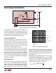
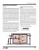
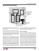
maximum rating. A ground plane should always be used
under the switcher circuitry to prevent interplane coupling
and overall noise.
The V
C
and FB components should be kept as far away as
possible from the switch and boost nodes. The LT1766
pinout has been designed to aid in this. The ground for
these components should be separated from the switch
current path. Failure to do so will result in poor stability
or subharmonic like oscillation.
Board layout also has a signifi cant effect on thermal
resistance. Pins 1, 8, 9 and 16, GND, are a continuous
copper plate that runs under the LT1766 die. This is the
best thermal path for heat out of the package. Reducing
the thermal resistance from Pins 1, 8, 9 and 16 onto the
board will reduce die temperature and increase the power
capability of the LT1766. This is achieved by providing as
much copper area as possible around these pins. Add-
ing multiple solder fi lled feedthroughs under and around
these four corner pins to the ground plane will also help.
Similar treatment to the catch diode and coil terminations
will reduce any additional heating effects. For the FE pack-
age, the exposed pad (Pin 17) should be soldered to the
copper ground plane underneath the device.
PARASITIC RESONANCE
Resonance or ringing may sometimes be seen on the
switch node (see Figure 7). Very high frequency ringing
following switch rise time is caused by switch/diode/input
capacitor lead inductance and diode capacitance. Schottky
diodes have very high “Q” junction capacitance that can
ring for many cycles when excited at high frequency. If
total lead length for the input capacitor, diode and switch
path is 1 inch, the inductance will be approximately 25nH.
At switch off, this will produce a spike across the NPN
output device in addition to the input voltage. At higher
currents this spike can be in the order of 10V to 20V
or higher with a poor layout, potentially exceeding the
abso
lute max switch voltage. The path around switch,
catch diode and input capacitor must be kept as short as
possible to ensure reliable operation. When looking at this,
Figure 6. Suggested Layout
GND GND
SHDN
SYNC
GND
BOOST
V
IN
SW
PLACE FEEDTHROUGH AROUND
GROUND PINS (4 CORNERS) FOR
GOOD THERMAL CONDUCTIVITY
LT1766
C3
C1
D1
C2
D2
R2
R1
1766 F06
C
FB
C
F
R
C
C
C
L1
MINIMIZE LT1766
C3-D1 LOOP
GND
GND
BIAS
FB
V
C
CONNECT TO
GROUND PLANE
KELVIN SENSE
V
OUT
KEEP FB AND V
C
COMPONENTS
AWAY FROM HIGH FREQUENCY,
HIGH CURRENT COMPONENTS
FOR THE FE PACKAGE, THE
EXPOSED PAD (PIN 17) SHOULD
BE PROPERLY SOLDERED TO
THE GROUND PLANE.
NOTE: BOOST AND BIAS
COPPER TRACES ARE ON
A SEPARATE LAYER FROM
THE GROUND PLANE
GND
V
OUT
V
IN
1
2
3
4
5
6
7
8
16
15
14
13
12
11
10
9