
Datasheet


LT1766/LT1766-5
9
1766fc
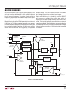
BLOCK DIAGRAM
will have 90° phase shift at a much lower frequency, but
will not have the additional 90° shift until well beyond
the LC resonant frequency. This makes it much easier to
frequency compensate the feedback loop and also gives
much quicker transient response.
Most of the circuitry of the LT1766 operates from an internal
2.9V bias line. The bias regulator normally draws power
from the regulator input pin, but if the BIAS pin is connected
to an external voltage higher than 3V, bias power will be
drawn from the external source (typically the regulated
–
+
–
+
–
+
–
+
∑
V
IN
2.9V BIAS
REGULATOR
200kHz
OSCILLATOR
FREQUENCY
FOLDBACK
SW
FB
GND
1, 8, 9, 16, 17
1766 F01
SLOPE COMP
ANTISLOPE COMP
BIAS
INTERNAL
V
CC
SYNC
0.4V
5.5μA
CURRENT
COMPARATOR
R
LIMIT
R
SENSE
ERROR
AMPLIFIER
g
m
= 2000μMho
Q2
FOLDBACK
CURRENT
LIMIT
CLAMP
BOOST
R
S
FLIP-FLOP
DRIVER
CIRCUITRY
S
R
Q1
POWER
SWITCH
1.22V
4
10
14
SHDN
15
6
2
12
11
V
C
LOCKOUT
COMPARATOR
SHUTDOWN
COMPARATOR
2.38V
×1
Q3
V
C(MAX)
CLAMP
output voltage). This will improve effi ciency if the BIAS
pin voltage is lower than regulator input voltage.
High switch effi ciency is attained by using the BOOST
pin to provide a voltage to the switch driver which is
higher than the input voltage, allowing switch to be satu-
rated. This boosted voltage is generated with an external
capacitor and diode. Two comparators are connected to the
shutdown pin. One has a 2.38V threshold for undervoltage
lockout and the second has a 0.4V threshold for complete
shutdown.
Figure 1. LT1766 Block Diagram