
Datasheet


1
LT1767/LT1767-1.8/
LT1767-2.5/LT1767-3.3/LT1767-5
sn1767 1767fas
Monolithic 1.5A, 1.25MHz
Step-Down Switching Regulators
■
1.5A Switch in a Small MSOP Package
■
Constant 1.25MHz Switching Frequency
■
High Power Exposed Pad (MS8E) Package
■
Wide Operating Voltage Range: 3V to 25V
■
High Efficiency 0.22Ω Switch
■
1.2V Feedback Reference Voltage
■
Fixed Output Voltages of 1.8V, 2.5V, 3.3V, 5V
■
2% Overall Output Tolerance
■
Uses Low Profile Surface Mount Components
■
Low Shutdown Current: 6µA
■
Synchronizable to 2MHz
■
Current Mode Loop Control
■
Constant Maximum Switch Current Rating at All Duty
Cycles*
The LT
®
1767 is a 1.25MHz monolithic buck switching
regulator. A high efficiency 1.5A, 0.22Ω switch is included
on the die together with all the control circuitry required to
complete a high frequency, current mode switching regu-
lator. Current mode control provides fast transient re-
sponse and excellent loop stability.
New design techniques achieve high efficiency at high
switching frequencies over a wide operating range. A low
dropout internal regulator maintains consistent perfor-
mance over a wide range of inputs from 24V systems to Li-
Ion batteries. An operating supply current of 1mA im-
proves efficiency, especially at lower output currents.
Shutdown reduces quiescent current to 6µA. Maximum
switch current remains constant at all duty cycles. Syn-
chronization allows an external logic level signal to in-
crease the internal oscillator from 1.4MHz to 2MHz.
The LT1767 is available in an 8-pin MSOP fused leadframe
package and a low thermal resistance exposed pad pack-
age. Full cycle-by-cycle short-circuit protection and ther-
mal shutdown are provided. High frequency operation
allows the reduction of input and output filtering compo-
nents and permits the use of chip inductors.
■
DSL Modems
■
Portable Computers
■
Wall Adapters
■
Battery-Powered Systems
■
Distributed Power
, LTC and LT are registered trademarks of Linear Technology Corporation.
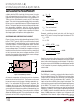
Efficiency vs Load Current
12V to 3.3V Step-Down Converter
BOOST
LT1767-3.3
V
IN
OUTPUT
3.3V
1.2A*
V
IN
12V
1767 TA01
C2
0.1µF
C
C
1.5nF
R
C
4.7k
D1
UPS120
C1
10µF
CERAMIC
C3
2.2µF
CERAMIC
D2
CMDSH-3
L1
5µH
V
SW
FBSHDN
OPEN
OR
HIGH
= ON
GND
V
C
SYNC
*MAXIMUM OUTPUT CURRENT IS SUBJECT TO THERMAL DERATING.
LOAD CURRENT (A)
0
0.2 0.4 0.6 0.8 1 1.2 1.4
EFFICIENCY (%)
1767 TA01a
95
90
85
80
75
70
V
IN
= 10V
V
OUT
= 5V
V
IN
= 5V
V
OUT
= 3.3V
*Patent Pending
APPLICATIO S
U
FEATURES
TYPICAL APPLICATIO
U
DESCRIPTIO
U