
Datasheet


13
LT1767/LT1767-1.8/
LT1767-2.5/LT1767-3.3/LT1767-5
sn1767 1767fas
APPLICATIONS INFORMATION
WUU
U
Notice that the catch diode’s forward voltage contributes
a significant loss in the overall system efficiency. A larger,
lower V
F
diode can improve efficiency by several percent.
P
INDUCTOR
= (I
LOAD
) (L
DCR
)
L
DCR
= Inductor DC resistance (assume 0.1Ω)
P
INDUCTOR
= (1) (0.1) = 0.1W
Typical thermal resistance of the board is 35°C/W. At an
ambient temperature of 65°C,
T
j
= 65 + 40 (0.4) + 35 (0.39) = 95°C
If a true die temperature is required, a measurement of the
SYNC to GND pin resistance can be used. The SYNC pin
resistance across temperature must first be calibrated,
with no device power, in an oven. The same measurement
can then be used in operation to indicate the die tempera-
ture.
FREQUENCY COMPENSATION
Before starting on the theoretical analysis of frequency
response, the following should be remembered – the
worse the board layout, the more difficult the circuit will be
to stabilize. This is true of almost all high frequency analog
circuits, read the ‘LAYOUT CONSIDERATIONS’ section
first. Common layout errors that appear as stability prob-
lems are distant placement of input decoupling capacitor
and/or catch diode, and connecting the V
C
compensation
to a ground track carrying significant switch current. In
addition, the theoretical analysis considers only first order
non-ideal component behavior. For these reasons, it is
important that a final stability check is made with produc-
tion layout and components.
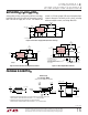
The LT1767 uses current mode control. This alleviates
many of the phase shift problems associated with the
inductor. The basic regulator loop is shown in Figure 7,
with both tantalum and ceramic capacitor equivalent cir-
cuits. The LT1767 can be considered as two g
m
blocks, the
error amplifier and the power stage.
Figure 8 shows the overall loop response with a 330pF V
C
capacitor and a typical 100µF tantalum output capacitor.
The response is set by the following terms:
Error amplifier:
DC gain set by g
m
and R
L
= 850µ • 500k␣ =␣ 425.
Pole set by C
F
and R
L
= (2π • 500k • 330p)
–1
= 965Hz.
Unity-gain set by C
F
and g
m
= (2π • 330p • 850µ
–1
)
–1
=
410kHz.
Power stage:
DC gain set by g
m
and R
L
(assume 10Ω) = 2.5 • 10 = 25.
Pole set by C
OUT
and R
L
= (2π • 100µ • 10)
–1
= 159Hz.
Unity-gain set by C
OUT
and g
m
= (2π • 100µ • 2.5
–1
)
–1
=
3.98kHz.
Tantalum output capacitor:
Zero set by C
OUT
and C
ESR
= (2π • 100µ • 0.1)
–1
= 15.9kHz.
Figure 8. Overall Loop Response
Figure 7. Model for Loop Response
–
+
1.2V
V
SW
V
C
LT1767
GND
1767 F07
R1
OUTPUT
ESR
C
F
C
C
R
C
500k
ERROR
AMPLIFIER
FB
R2
C1
CURRENT MODE
POWER STAGE
g
m
= 2.5mho
g
m
=
850µmho
+
ESL
CERAMICTANTALUM
C1
FREQUENCY (Hz)
GAIN (dB)
80
60
40
20
0
–20
–40
PHASE (DEG)
180
150
120
90
60
30
0
1767 F10
GAIN
PHASE
V
OUT
= 5V
C
OUT
= 100µF, 0.1Ω
C
C
= 330pF
R
C
/C
F
= N/C
I
LOAD
= 500mA
10 1k 10k 1M100 100k