
Datasheet


LT1768
12
APPLICATIONS INFORMATION
WUU
U
and is dependant on the operating mode. For dual lamp
displays, the transfer function for minimum current mode
(I
DIO
/I
RMIN
) is equal to 10A/A, and for maximum current
mode (I
DIO
/I
RMAX
) is equal to 100A/A.
The transfer functions discussed above are between R
MAX
and R
MIN
current and average lamp current
not
RMS lamp
current. Due to the differences between the average and
RMS functions, the actual overall transfer function be-
tween actual lamp current and R
MIN
/R
MAX
current must be
empirically determined, and is dependant on the particular
lamp/display housing combination used. For example, in
the circuit of Figure 1 setting R
RMIN
to 10kΩ and R
RMAX
to
16.8Ω, sets the minimum and maximum RMS lamp
currents for the example display to 1mA and 9mA per lamp
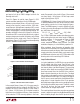
respectively. Figure 4 shows the lamp current vs program-
ming voltage for the circuit in Figure 1.
R
RMIN
adjusted to produce the specified current. If a wide
dimming range is desired, V
PROG
should be set to 0.75V
and R
RMIN
adjusted to produce the required dimming
ratio. Care must be taken when adjusting R
RMIN
to pro-
duce extreme dimming ratios. The minimum lamp current
set by R
RMIN
must be able to fully illuminate the lamp or
thermometering (uneven illumination) will occur. If the
desired dimming ratio can’t be achieved by adjusting
R
RMIN
, the minimum lamp current can be set to zero by
connecting the R
MIN
pin to the V
REF
pin. If the minimum
current is set to less than the open lamp threshold current
(approximately 125µA), the FAULT pin will be activated for
PROG voltages between 0.5V and 1V.
The values chosen for R
RMAX
and R
RMIN
are extremely
critical in determining the lifetime of the display. It is
imperative that proper measurement techniques, such as
those cited in the references, be used when determining
R
RMAX
and R
RMIN
values.
Lamp Fault Modes and Single Lamp Operation
The DIO pin diodes that conduct on the positive cycle are
used to detect open lamp fault conditions. If the current
in either of the DIO pins on the positive half cycle is less
than 125µA due to either an open lamp or lamp lowside
short to ground, for a minimum of 1 PWM cycle, then the
FAULT pin will be activated and the lamp programming
current into the VC pin in high level PWM mode, linear
mode, and maximum current mode, will be reduced by
approximately 50%. Halving the VC source current will cut
the total lamp current to approximately one half of its
programmed value. This function insures that the maxi-
mum lamp current level set by R
RMAX
will not be exceeded
even under fault conditions. If the current in both of the
DIO pins on the positive cycle is less than 125µA, and the
VC pin hits its clamp value (indicating an open lamp or
lamp lowside short to ground fault condition) for a mini-
mum of 1 PWM cycle, the gate drive will be latched off. The
latch can be cleared by setting the PROG voltage to zero or
placing the LT1768 in shutdown mode.
Since open lamp fault conditions produce high voltage AC
waveforms, it is imperative that proper layout spacings
between the high voltage and DIO lines be observed.
Coupling capacitance as low as 0.5pF between the high
Figure 4. Lamp Current vs PROG Voltage for
the Circuit in Figure 1
Choosing R
RMAX
and R
RMIN
and V
PWM
The value for R
RMAX
should be determined by setting
V
PROG
to 4.5V then adjusting R
RMAX
to produce the
maximum allowable current specified by the lamp manu-
facturer.
The voltage for the PWM pin should then be set so that the
LT1768 normally operates in linear mode. A typical value
for V
PWM
is approximately 2.5V, which limits the PWM
region to 50% of the V
PROG
input voltage range.
The value for R
RMIN
should be chosen to either produce
the minimum manufacturer specified lamp current or
enable a wide dimming range. If a minimum specified
current is desired, the V
PROG
should be set to 0.75V and
V
PROG
(V)
1.00.5
5.04.03V (V
PWM)
MIN
CURRENT
PWM
(FREQ = 220Hz)
MAX
CURRENTLINEAR
0%
100%
OFF
9mA
6mA
0mA
I
CCFL
(mA)
1768 F04