
Datasheet


LT1768
14
up current source. The LT1768 thermal shutdown tem-
perature is set at 160°C. A buffered version of the internal
5V is present at the V
REF
pin and is capable of supplying up
to 10mA of current. Note that using any substantial
amount of current from the V
REF
pin will increase power
dissipation in the device, which will reduce the useful
operating ambient temperature range.
Supply and Input Voltage Sequencing
For most applications, where the SHDN pin is left floating,
and the voltages on the PWM and PROG pins are derived
from the V
REF
pin, the LT1768 will power-up and power-
down correctly when the voltage to the V
IN
pin is applied
and removed. In applications where the voltage inputs for
the V
IN
pin, SHDN pin, PWM pin, and the PROG pin
originate from different sources (power supply, micropro-
cessors etc.), care must be taken during power up/down
sequences. For proper operation during the power-up
sequence, the voltage on the following pins must be taken
from zero to their appropriate values in the following
order; V
IN
pin, SHDN pin, PWM pin and PROG pin. For
proper operation during the power-down sequence, the
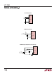
order must be reversed. For example, in the circuit of
Figure 1 where the SHDN pin is left floating, and the PWM
pin voltage is derived from a resistor divider to the V
REF
pin, the proper power-up sequence would be to take the
V
IN
pin from zero to its value then apply either a voltage or
PWM signal to the PROG pin. The power-down sequence
for the circuit in Figure 1 would be to take the PROG pin
voltage to zero, then take the V
IN
pin voltage to zero.If the
PROG voltage in the circuit of Figure 1 is present before the
V
IN
supply voltage, proper power supply sequecing can be
achieved by implementing the circuit shown in Figure 7.
APPLICATIONS INFORMATION
WUU
U
1768 • G06
PGND
GATE
BAT 85
LT1768
GATE
The LT1768 has a single high current totem pole output
stage. This output stage is capable of driving up to ±1.5A
of output current. Cross-conduction current spikes in the
totem pole output have been eliminated. The GATE pin is
intended to drive an N-channel MOSFET switch. Rise and
fall times are typically 50ns with a 3000pF load. A clamp
is built into the device to prevent the GATE pin from rising
above 13V in order to protect the gate of the MOSFET
switch.
The GATE pin connects directly to the emitter of the upper
NPN drive transistor and the collector of the lower NPN
drive transistor in the totem pole. The collector of the lower
transistor, which is N-type silicon, forms a P-N junction
with the substrate of the device. This junction is reversed
biased during normal operation.
In some applications the parasitic LC of the external
MOSFET gate can ring and pull the GATE pin below
ground. If the GATE pin is pulled negative by more than a
diode drop the parasitic diode formed by the collector of
the GATE NPN and the substrate will turn on. This can
cause erratic operation of the device. In these cases a
Schottky clamp diode is recommended from the GATE pin
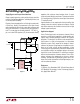
to ground. (Figure 6.)
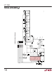
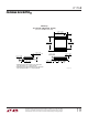
Figure 6. Schottky Gate Clamp
49.9k
10k
10µF
0 TO 5V
OR
1kHz PWM
VN2222LL
1768 F07
V
IN
PROG
LT1768
Figure 7. Circuit Insures Proper Supply Sequencing When
Dimming Voltage Exists Before Main Power Supply
Reference
The internal reference of the LT1768 is a trimmed bandgap
reference. The reference is used to power the majority of
the LT1768 internal circuitry. The reference is inactive if
the LT1768 is in undervoltage lockout, shutdown mode, or
thermal shutdown. The undervoltage lockout is active
when V
IN
is below 7.9V and the LT1768 is in shutdown
mode when the voltage on the SHDN pin is pulled below
1V. The SHDN pin has 200mV of hysteresis and a 7µA pull-