
Datasheet


14
LT1769
1769fa
APPLICATIONS INFORMATION
WUU
U
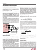
Figure 11. Replacing the Input Diode
CHARGE CURRENT (A)
0
LEAD TEMPERATURE ON PINS 1, 2, 3 (°C)
40
50
2
1769 F09
30
20
0.5
1
1.5
70
60
NOTE: PEAK DIE TEMPERATURE
WILL BE ABOUT 15°C HIGHER AT
2A CHARGE CURRENT
V
IN
= 19V
V
BAT
= 12.3V
V
BOOST
= 5V
2-LAYER BOARD
ROOM TEMP = 24°C
5 IN
2
BOARD
25 IN
2
BOARD
BOARD AREA (IN
2
)
0
45
40
35
30
25
20
15
10
15 25
1769 F08
510
20 30 35
THERMAL RESISTANCE (°C/W)
MEASURED FROM AIR AMBIENT
TO DIE USING COPPER LANDS
AS SHOWN ON DATA SHEET
2-LAYER BOARD
4-LAYER BOARD
Figure 8. LT1769 Thermal Resistance
Figure 10. High Duty Cycle
V
IN
SW
BOOST
SPIN
SENSE BAT
V
CC
V
X
3V TO 6V
C
X
10µF
V
BAT
1769 F11
C2
0.47µF
D2
D1
R
X
50k
Q2
Q1
LT1769
HIGH DUTY CYCLE CONNECTION
Q1 = Si4435DY
Q2 = TP0610L
+
+
SW
BOOST
SPIN
SENSE BAT
V
BAT
C3
0.47µF
D2
LT1769
SW
BOOST
SPIN
SENSE BAT
V
X
3V TO 6V
C
X
10µF
V
BAT
1769 F10
C3
0.47µF
D2
LT1769
STANDARD CONNECTION HIGH DUTY CYCLE CONNECTION
+ +
an 18V ±3% adapter is used to charge ten NiMH cells, the
charger must put out approximaly 15V. A total of 1.6V is
lost in the input diode, switch resistance, inductor resis-
tance and parasitics, so the required duty cycle is
15/16.4 = 91.4%. The duty cycle can be extended to 93%
by restricting boost voltage to 5V instead of using V
BAT
as
is normally done. This lower boost voltage also reduces
power dissipation in the LT1769, so it is a win-win
decision. Connect an external source of 3V to 6V at V
X
node in Figure 10 with a 10µF C
X
bypass capacitor.
Lower Dropout Voltage
For even lower dropout and/or reducing heat on the board,
the input diode D3 can be replaced with a FET (see Figure
11). Connect a P-channel FET in place of the input diode
with its gate connected to the battery causing the FET to
turn off when the input voltage goes low. The problem is
that the gate must be pumped low so that the FET is fully
turned on even when the input is only a volt or two above
the battery voltage. Also there is a turn-off speed issue.
The FET should turn off instantly when the input is dead
shorted to avoid large current surges from the battery
back through the charger into the FET. Gate capacitance
slows turn-off, so a small P-channel (Q2) is added to
discharge the gate capacitance quickly in the event of an
input short. The Q2 body diode creates the necessary
pumping action to keep the gate of Q1 low during normal
operation. Note that Q1 and Q2 have a V
GS
spec limit of
20V. This restricts V
IN
to a maximum of 20V. For low
dropout operation with V
IN
> 20V consult factory.
Figure 9. LT1769 Lead Temperature