
Datasheet


8
LT1769
1769fa
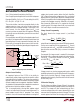
TEST CIRCUITS
Test Circuit 1
–
+
V
REF
≈ 0.65V
V
BAT
V
C
CA2
–
+
–
+
CA1
+
300Ω
20k
1k
1k
R
S1
100Ω
BAT
SENSE
SPIN
1769 TC01
PROG
R
PROG
0.047µF
LT1769
1µF
60k
LT1006
+
R
S2
200Ω
R
S3
200Ω
Test Circuit 2
V
REF
2.465V
–
+
+
10k
10k
OVP
1769 TC02
I
PROG
R
PROG
LT1769
PROG
LT1013
0.47µF
–
+
VA
OPERATION
U
The LT1769 is a current mode PWM step-down (buck)
switcher. The battery DC charge current is programmed
by a resistor R
PROG
(or a DAC output current) at the PROG
pin (see Block Diagram). Amplifier CA1 converts the
charge current through R
S1
to a much lower current I
PROG
fed into the PROG pin. Amplifier CA2 compares the output
of CA1 with the programmed current and drives the PWM
control loop to force them to be equal. High DC accuracy
is achieved with averaging capacitor C
PROG
. Note that
I
PROG
has both AC and DC components. I
PROG
goes
through R1 and generates a ramp signal that is fed to the
PWM control comparator C1 through buffer B1 and level
shift resistors R2 and R3, forming the current mode inner
loop. The BOOST pin drives the switch NPN Q
SW
into
saturation and reduces power loss. For batteries like
lithium-ion that require both constant-current and con-
stant-voltage charging, the 0.5%, 2.465V reference and
the amplifier VA reduce the charge current when battery
voltage reaches the preset level. For NiMH and NiCd, VA
can be used for overvoltage protection. When the input
voltage is removed, the V
CC
pin drops to 0.7V below the
battery voltage, forcing the charger into a low battery drain
(3µA typical) sleep mode. To shut down the charger,
simply pull the V
C
pin low with a transistor.